Wave-absorbing shielding adhesive film and preparation method thereof

A technology of adhesive film and adhesive film layer, applied in the direction of magnetic field/electric field shielding, adhesive, film/sheet adhesive, etc., can solve the problem of demanding product thickness, unsatisfactory thickness and absorption frequency, complex interference of electromagnetic waves and Serious problems, to achieve the effect of suppressing electronic noise

Inactive Publication Date: 2020-07-14
SUZHOU VERYBOND MATERIALS CO LTD
View PDF13 Cites 1 Cited by
  • Summary
  • Abstract
  • Description
  • Claims
  • Application Information

AI Technical Summary

Problems solved by technology

[0002] With the development of electronic equipment such as notebook computers, monitors, mobile phones and tablet computers, which are becoming thinner and more highly integrated, the mutual interference of electromagnetic waves in various frequency bands between electronic components inside them is becoming more and more complicated and serious. Conventional shielding materials such as tape, conductive foam, and metal foil can no longer meet the needs of this complex and changeable use environment. At the same time, the requirements for product thickness are becoming more and more stringent. Materials put forward higher requirements
Especially in the design and production of ultra-thin LCD, LED, OLED, Micro-LED and Mini-LED, it is even more so to prevent the electromagnetic waves of internal components and external equipment from interfering with its display effect, and the requirements for new composite shielding materials are even higher. Urgent, for the existing conductive cloth, conductive foam and metal foil and other products can not fully and effectively solve the various electronic clutter and electronic Noise interference, and at the same time, the thickness and absorption frequency cannot meet the requirements of specific frequencies

Method used


Image

  • Wave-absorbing shielding adhesive film and preparation method thereof
  • Wave-absorbing shielding adhesive film and preparation method thereof
  • Wave-absorbing shielding adhesive film and preparation method thereof

Examples


Embodiment Construction

[0023] The present invention will be further described below in conjunction with the accompanying drawings and specific embodiments, so that those skilled in the art can better understand the present invention and implement it, but the examples given are not intended to limit the present invention.

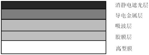
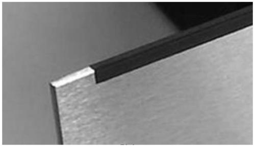
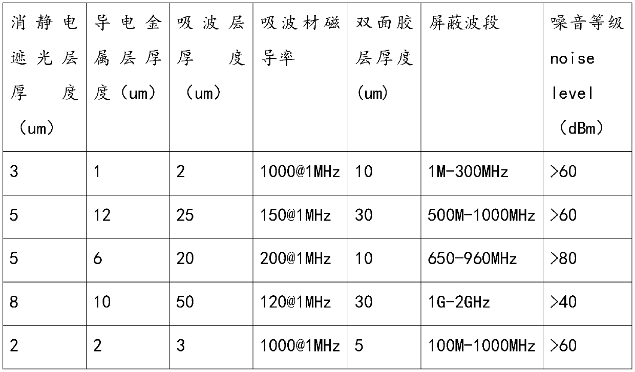
[0024] refer to Figure 1-Figure 2 As shown, the present invention discloses a wave-absorbing shielding adhesive film, which includes an adhesive film layer, a wave-absorbing layer, a conductive metal layer, and a static-dissipating light-shielding layer arranged in sequence. The wave-absorbing layer is made of a soft magnetic alloy material, and the static-dissipating light-shielding layer is Conductive ink or polyimide.

[0025] The conductive metal layer can be copper foil, which has better shielding performance and better thermal conductivity than metal foils such as aluminum foil. The thickness of the conductive metal layer can be 1-50um.

[0026] The adhesive film can be a...


PUM


Abstract

The invention discloses a wave-absorbing shielding adhesive film and a preparation method thereof, the wave-absorbing shielding adhesive film comprises an adhesive film layer, a wave-absorbing layer,a conductive metal layer and an anti-static shading layer which are arranged in sequence, the wave-absorbing layer is made of a soft magnetic alloy material, and the anti-static shading layer is madeof conductive ink or polyimide; the preparation method comprises the following steps: taking a conductive metal layer as a substrate, coating one surface of the conductive metal layer with an anti-static shading layer, and then performing drying; coating the other surface of the conductive metal layer with a soft magnetic alloy material, and performing multi-roller hot pressing and curing to obtain an absorption layer; and coating pressure-sensitive glue on the absorption layer, and drying, curing and forming a film to obtain an adhesive film layer. Effective shielding can be achieved under the ultra-thin thickness, and therefore electromagnetic wave interference resistance and electronic noise suppression are achieved.

Description

technical field [0001] The invention relates to the technical field of electromagnetic shielding, in particular to a wave-absorbing shielding adhesive film and a preparation method thereof. Background technique [0002] With the development of electronic equipment such as notebook computers, monitors, mobile phones and tablet computers, which are becoming thinner and more highly integrated, the mutual interference of electromagnetic waves in various frequency bands between electronic components inside them is becoming more and more complicated and serious. Conventional shielding materials such as tape, conductive foam, and metal foil can no longer meet the needs of this complex and changeable use environment. At the same time, the requirements for product thickness are becoming more and more stringent. Materials put forward higher requirements. Especially in the design and production of ultra-thin LCD, LED, OLED, Micro-LED and Mini-LED, it is even more so to prevent the ele...

Claims


Application Information

Patent Timeline
Patent Type & Authority Applications(China)
IPC IPC(8): C09J7/28C09D11/52C09D5/24C09D179/08H05K9/00
CPCC09D5/24C09D11/52C09D179/08C09J2400/16C09J2400/163C09J2433/00C09J2479/00C09J7/28H05K9/0084
Inventor 张立伟赵立萍张立涛
Owner SUZHOU VERYBOND MATERIALS CO LTD
Why Eureka
Try Eureka