Fabrication method of double-layer silicon-based filter based on three-dimensional inductor

A manufacturing method and filter technology, which are applied to semiconductor devices, waveguide-type devices, electric solid-state devices, etc., can solve the problems of low integration density and large size of filters, and achieve the effect of batch production and improved production efficiency.

Active Publication Date: 2021-10-15
THE 13TH RES INST OF CHINA ELECTRONICS TECH GRP CORP
View PDF5 Cites 0 Cited by
  • Summary
  • Abstract
  • Description
  • Claims
  • Application Information

AI Technical Summary

Problems solved by technology

[0003] In view of this, the embodiment of the present invention provides a method for manufacturing a double-layer silicon-based filter based on a three-dimensional inductor, so as to solve the problem in the prior art that the integration density of the filter is not high, resulting in a slightly larger size

Method used


Image

  • Fabrication method of double-layer silicon-based filter based on three-dimensional inductor
  • Fabrication method of double-layer silicon-based filter based on three-dimensional inductor
  • Fabrication method of double-layer silicon-based filter based on three-dimensional inductor

Examples


Embodiment Construction

[0048] In the following description, specific details such as specific system structures and technologies are presented for the purpose of illustration rather than limitation, so as to thoroughly understand the embodiments of the present invention. It will be apparent, however, to one skilled in the art that the invention may be practiced in other embodiments without these specific details. In other instances, detailed descriptions of well-known systems, devices, circuits, and methods are omitted so as not to obscure the description of the present invention with unnecessary detail.

[0049] In order to illustrate the technical solutions of the present invention, specific examples are used below to illustrate.

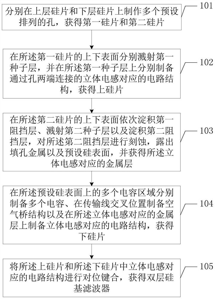
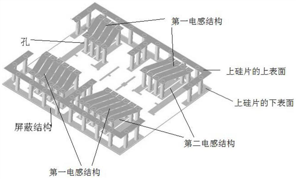
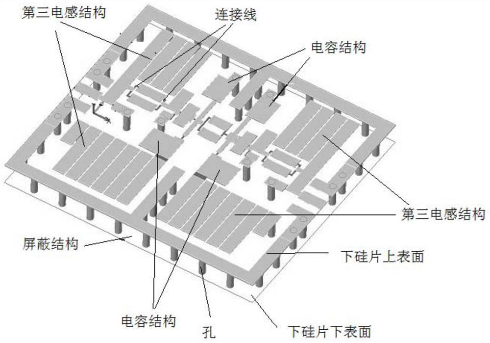
[0050] figure 1 The implementation flow diagram of the manufacturing method of the double-layer silicon-based filter based on the three-dimensional inductance provided by the embodiment of the present invention is described in detail as follows.

[0051] Step 101 , ma...


PUM


Abstract

The present invention is applicable to the field of filter manufacturing technology, and provides a method for manufacturing a double-layer silicon-based filter based on a three-dimensional inductor. The method includes: preparing a circuit structure corresponding to the three-dimensional inductor on the upper silicon chip, Prepare multiple capacitors, prepare an air bridge structure at the crossing position of the transmission line, and prepare a circuit structure corresponding to the three-dimensional inductance on the metal layer corresponding to the three-dimensional inductance, and align the circuit structure corresponding to the three-dimensional inductance in the upper silicon chip and the lower silicon chip Bonding to obtain a double-layer silicon-based filter, so that a smaller-sized double-layer silicon-based filter based on a three-dimensional inductor can be obtained, and no manual intervention is required in the process of manufacturing a double-layer silicon-based filter based on a three-dimensional inductor. Therefore, batch production can be realized and production efficiency can be improved.

Description

technical field [0001] The invention belongs to the technical field of filter production, and in particular relates to a production method of a double-layer silicon-based filter based on a three-dimensional inductance. Background technique [0002] As an important component in the millimeter wave communication system, the filter has become an important research direction for miniaturization. The size of the microwave filter should be reduced as much as possible, and it can be connected and integrated with other modules as conveniently and flexibly as possible, so as to promote the integration of the microwave system as a whole. miniaturization and portability. However, the size of existing filters is on the order of centimeters, and the integration density is not high, resulting in a slightly larger size. Contents of the invention [0003] In view of this, an embodiment of the present invention provides a method for manufacturing a double-layer silicon-based filter based ...

Claims


Application Information

Patent Timeline
Patent Type & Authority Patents(China)
IPC IPC(8): H01P1/20H01L23/64
CPCH01L23/645H01P1/20
Inventor 董春晖杨志商庆杰丁现朋张晓磊王敬轩李丰钱丽勋李海剑李宏军
Owner THE 13TH RES INST OF CHINA ELECTRONICS TECH GRP CORP
Why Eureka
Try Eureka