Unlock instant, AI-driven research and patent intelligence for your innovation.

A peripheral circuit and three-dimensional memory

A peripheral circuit and memory technology, applied in circuits, electrical solid devices, electrical components, etc., can solve the problem of not being able to share a region well area connection, etc., and achieve the effect of improving electrical performance and integration.

Active Publication Date: 2021-06-08
YANGTZE MEMORY TECH CO LTD
View PDF3 Cites 0 Cited by
  • Summary
  • Abstract
  • Description
  • Claims
  • Application Information

AI Technical Summary

Problems solved by technology

[0003] The present application provides a peripheral circuit and a three-dimensional memory, which solves the problem in the prior art that adjacent field effect transistors of the peripheral circuit cannot share a region of well connection

Method used


Image

  • A peripheral circuit and three-dimensional memory
  • A peripheral circuit and three-dimensional memory
  • A peripheral circuit and three-dimensional memory

Examples


Embodiment Construction

[0025] The following will clearly and completely describe the technical solutions in the embodiments of the application with reference to the drawings in the embodiments of the application. Apparently, the described embodiments are only some of the embodiments of the application, not all of them. Based on the embodiments in this application, all other embodiments obtained by persons of ordinary skill in the art without creative efforts fall within the protection scope of this application.

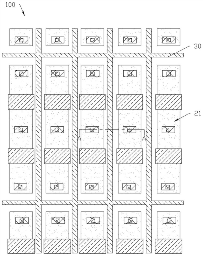
[0026] As word lines and bit lines of a memory array become denser in a three-dimensional memory, the size of peripheral circuits and the spacing between adjacent semiconductor devices on the peripheral circuits become smaller and smaller. At the same time, a higher voltage is applied to operate a three-dimensional memory with higher density and larger storage capacity. Therefore, there are challenges to maintaining the desired reliability of semiconductor devices in three-dimensional memor...


PUM


Abstract

The present application provides a peripheral circuit and a three-dimensional memory, the peripheral circuit includes a plurality of semiconductor device groups arranged in an array, and the distance between two adjacent columns of the semiconductor device groups arranged at intervals in the first direction of the peripheral circuit and Bottom isolation is provided between two adjacent rows of the semiconductor device groups arranged at intervals in the second direction of the peripheral circuit, the first direction and the second direction are perpendicular to realize the adjacent semiconductor device groups Electrical isolation of device groups, a connection structure is provided between two adjacent groups of semiconductor device groups in the first direction, and the connection structure is used to connect adjacent semiconductor device groups in the first direction The first type well region. The peripheral circuit provided by the present application solves the problem in the prior art that adjacent field effect transistors of the peripheral circuit cannot share a region of well connection.

Description

technical field [0001] The invention belongs to the technical field of semiconductor components, and in particular relates to a peripheral circuit and a three-dimensional memory. Background technique [0002] As people's requirements for electronic products are developing towards miniaturization, the requirements for the integration of three-dimensional memory are getting higher and higher. In the prior art, the peripheral circuit of the three-dimensional memory isolates a single field effect transistor in the field effect transistor (metal oxide semiconductor, MOS) array of the peripheral circuit in pursuit of integration, but isolating each field effect transistor will cause adjacent Field effect transistors cannot share a region of the well connection. Contents of the invention [0003] The present application provides a peripheral circuit and a three-dimensional memory, which solves the problem in the prior art that adjacent field effect transistors of the peripheral ...

Claims


Application Information

Patent Timeline
Patent Type & Authority Patents(China)
IPC IPC(8): H01L27/11519H01L27/11526H01L27/11551H01L27/11565H01L27/11573H01L27/11578H10B41/10H10B41/20H10B41/40H10B43/10H10B43/20H10B43/40
CPCH10B41/10H10B41/40H10B41/20H10B43/10H10B43/40H10B43/20
Inventor 许文山刘威
Owner YANGTZE MEMORY TECH CO LTD