Surface protectant for semiconductor wafer

A surface protectant, semiconductor technology, applied in the manufacture of semiconductor/solid state devices, surface etching compositions, polishing compositions containing abrasives, etc., can solve the problems of scratches, scratches, easy agglomeration, etc. , The effect of reducing scratches, high flatness and low defects

Active Publication Date: 2020-08-07
DAICEL CHEM IND LTD
View PDF11 Cites 0 Cited by
  • Summary
  • Abstract
  • Description
  • Claims
  • Application Information

AI Technical Summary

Problems solved by technology

However, fine abrasives are easy to aggregate, and there is a problem that scratches (scratches) are easily generated on the surface of the semiconductor wafer due to the aggregates of the abrasives.

Method used


Image

  • Surface protectant for semiconductor wafer
  • Surface protectant for semiconductor wafer
  • Surface protectant for semiconductor wafer

Examples


Embodiment 1

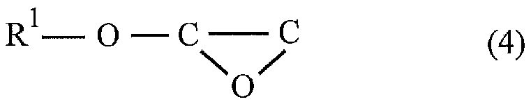
[0086] 4 mol of 2,3-epoxy-1-propanol (trade name "Glycidol", manufactured by Daicel Co., Ltd.) was added to 1 mol of lauryl alcohol to obtain compound (A1) (C 12 h 25 O-(C 3 h 6 o 2 ) 4 -H, molecular weight: 482).

[0087] The obtained compound (A1) was diluted with water so that the concentration of the obtained compound (A1) became 15% by weight, and a semiconductor wafer surface protective agent (A1) was obtained.

Embodiment 2

[0089] The consumption of 2,3-epoxy-1-propanol was changed to 10mol, except that, compound (A2) was obtained in the same manner as in Example 1 (C 12 h 25 O-(C 3 h 6 o 2 ) 10 -H, molecular weight: 926).

[0090] The obtained compound (A2) was diluted with water so that the concentration of the obtained compound (A2) became 15 weight%, and the semiconductor wafer surface protective agent (A2) was obtained.

Embodiment 3

[0092] The consumption of 2,3-epoxy-1-propanol was changed to 6mol, except that, compound (A3) was obtained in the same manner as in Example 1 (C 12 h 25 O-(C 3 h 6 o 2 ) 6 -H, molecular weight: 630).

[0093] The obtained compound (A3) was diluted with water so that the concentration of the obtained compound (A3) became 15 weight%, and the semiconductor wafer surface protective agent (A3) was obtained.


PUM


Abstract

Provided is a surface protectant which suppresses corrosion of the surface of a semiconductor wafer by an alkaline compound, thereby reducing defects in the semiconductor wafer. The semiconductor wafer surface protectant contains a compound represented by formula (1): R<1>O-(C3H6O2)<n>-H (1). In the formula, R1 represents a hydrogen atom, a hydrocarbon group with carbon number of 1-24 optionally having a hydroxyl group, or a group represented by R2CO, R2 represents a hydrocarbon group with the carbon number of 1-24, and n represents the average degree of polymerization of the glycerin unit represented in the bracket and is 2-60.

Description

technical field [0001] The present invention relates to a surface protective agent for semiconductor wafers. This application claims the priority of Japanese Patent Application No. 2019-013877 filed in Japan on January 30, 2019, the contents of which are incorporated herein by reference. Background technique [0002] In recent years, semiconductor devices tend to be miniaturized and highly integrated. Among them, the wiring layer in which circuits are formed on the surface of the semiconductor wafer is required to be highly planarized on the surface of the semiconductor wafer in order to prevent interruption of the wiring and increase the local resistance value while stacking as designed. [0003] CMP (Chemical Mechanical Planarization) has been widely used as a planarization technique for the surface of the above-mentioned semiconductor wafer. CMP is a technique for eliminating level differences on the surface of a semiconductor wafer through both chemical action by the b...

Claims


Application Information

Patent Timeline
Patent Type & Authority Applications(China)
IPC IPC(8): C09G1/02H01L21/306
CPCC09G1/02H01L21/30625C08G65/2609C09D171/02H01L21/02024H01L21/306C09K3/14C09D163/00C09D5/08C09K13/02H01L21/02013H01L21/302
Inventor 坂西裕一
Owner DAICEL CHEM IND LTD
Why Eureka
Try Eureka