
Photoetching mask optimization method and device for graphic image joint optimization and electronic equipment

A joint optimization, graphics and image technology, which is applied to the exposure device of the photoplate making process, the photoplate making process of the pattern surface, optics, etc., can solve the problem of unsatisfactory imaging of the mask plate, and achieve the effect of improving the final optimization effect and avoiding deviation

Active Publication Date: 2020-08-07
SHENZHEN JINGYUAN INFORMATION TECH CO LTD
View PDF4 Cites 0 Cited by
  • Summary
  • Abstract
  • Description
  • Claims
  • Application Information

AI Technical Summary

Problems solved by technology

[0004] In order to overcome the problem that the existing mask optimization technology is limited by the influence of the grid point position, resulting in unsatisfactory imaging of the optimized mask template, the present invention provides a photolithography mask optimization method, device and electronic equipment for joint optimization of graphics and images

Method used


Image

  • Photoetching mask optimization method and device for graphic image joint optimization and electronic equipment
  • Photoetching mask optimization method and device for graphic image joint optimization and electronic equipment
  • Photoetching mask optimization method and device for graphic image joint optimization and electronic equipment

Examples


Embodiment approach

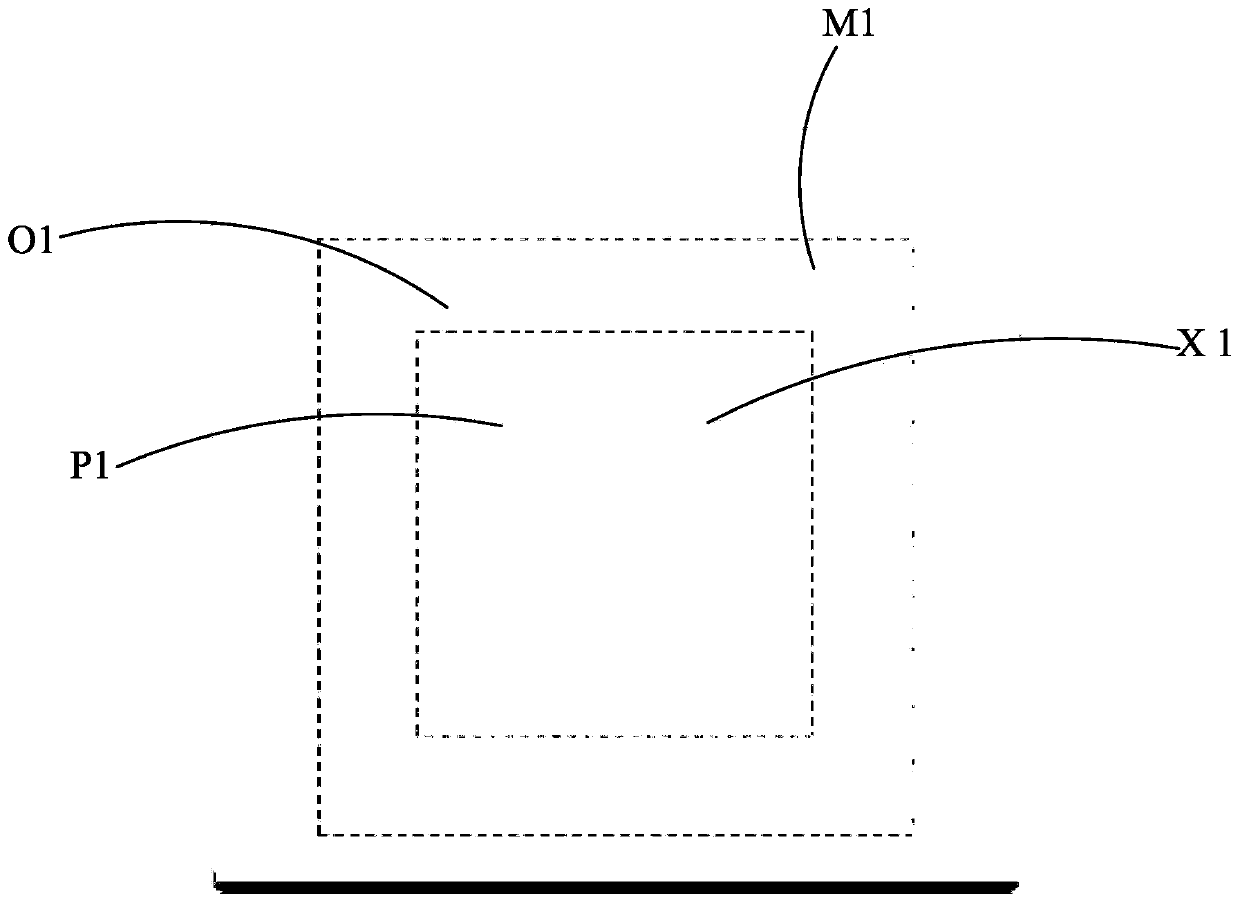
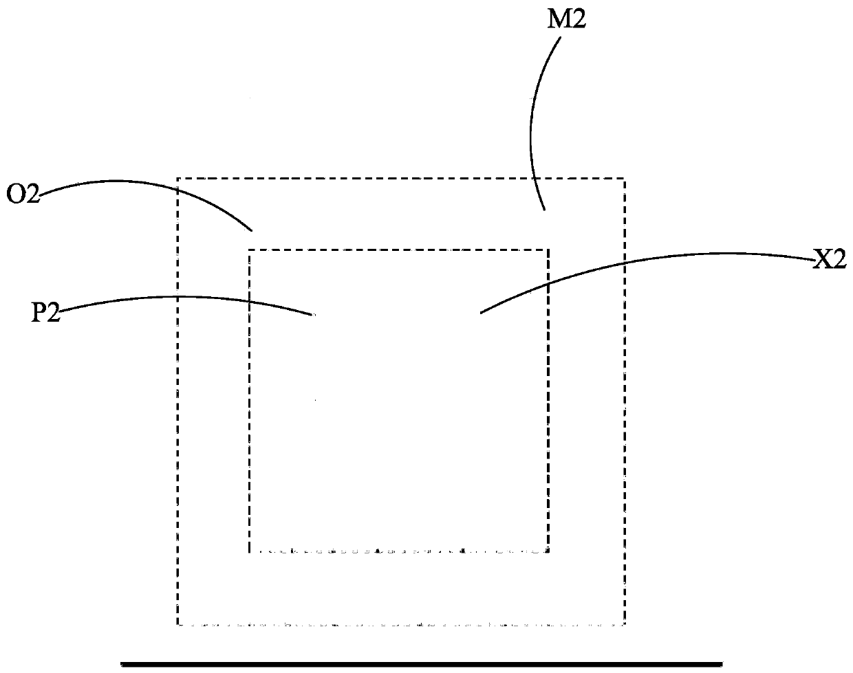
[0051] In order to eliminate the influence of the optical proximity effect, the main pattern on the initial mask is different from the desired lithographic pattern, and the main pattern needs to be processed by Optical Proximity Correction (OPC, Optical Proximity Correction). In the range of 90nm, the line width of the main pattern is even only 1 / 3 of the light wavelength. In addition to the above-mentioned necessary optical proximity correction processing, it is usually necessary to set sub-size auxiliary patterns around the main pattern, that is, sub-resolution auxiliary patterns. Technology (SRAF, Sub-resolution assistant feature). These auxiliary patterns are only set on the photolithographic mask, and the patterns will not be transferred to the semiconductor device after the actual exposure, but only increase the depth of focus adjacent to the main pattern and improve the exposure accuracy. Therefore, in this step, the auxiliary graphics placement area is an area for plac...


PUM


Abstract

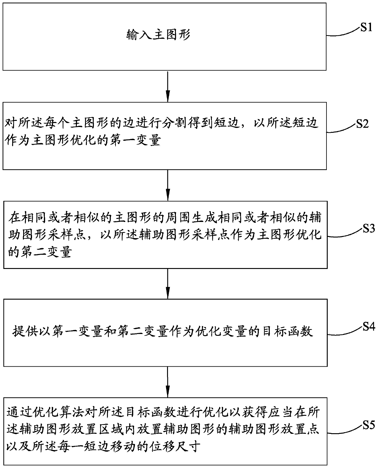
The invention relates to the field of integrated circuit mask design, in particular to a photoetching mask optimization method and device for graphic image joint optimization and electronic equipment.The method comprises the following steps: inputting a main graph; segmenting the edge of the main graph to obtain a short edge, and taking the short edge as a first variable for optimizing the main graph; generatingsame or similar auxiliary graph sampling points around the same or similar main graphs, and taking the auxiliary graph sampling points as second variables for main graph optimization;providinga target function taking a first variable and a second variable as optimization variables, wherein rules for generating auxiliary graph sampling points around each main graph are the same andare not limited by specific positions of the main graphs, so thatconsistency of optimization results of each main graph is guaranteed finally.

Description

【Technical field】 [0001] The invention relates to the field of integrated circuit mask design, in particular to a photolithography mask optimization method, device and electronic equipment for joint optimization of graphics and images. 【Background technique】 [0002] Photolithography is one of the most important parts of the integrated circuit manufacturing process, which determines the advanced level of the integrated circuit manufacturing process. A lithography system is usually described as an optical imaging system, including four basic elements: an illumination source, a mask, a projection objective lens system, and a silicon wafer coated with photoresist. As the key dimensions of integrated circuits enter the 45nm technology node, and continue to move towards a smaller size of 32nm or even 22nm nodes, the size of the pattern that needs to be exposed is much smaller than the wavelength of the light source in the lithography system. In this case, the optical proximity e...

Claims


Application Information

Patent Timeline
Patent Type & Authority Applications(China)
IPC IPC(8): G06F30/398
CPCG06F30/398G03F1/36G03F7/20G03F1/70
Inventor 丁明施伟杰
Owner SHENZHEN JINGYUAN INFORMATION TECH CO LTD
Learn More