Semiconductor crystal growth device

A crystal growth and semiconductor technology, applied in the direction of crystal growth, single crystal growth, single crystal growth, etc., to achieve the effect of increasing the axial temperature gradient, improving the quality of crystal pulling, and reducing the difference

Active Publication Date: 2020-08-11
ZING SEMICON CORP
View PDF4 Cites 2 Cited by
  • Summary
  • Abstract
  • Description
  • Claims
  • Application Information

AI Technical Summary

Problems solved by technology

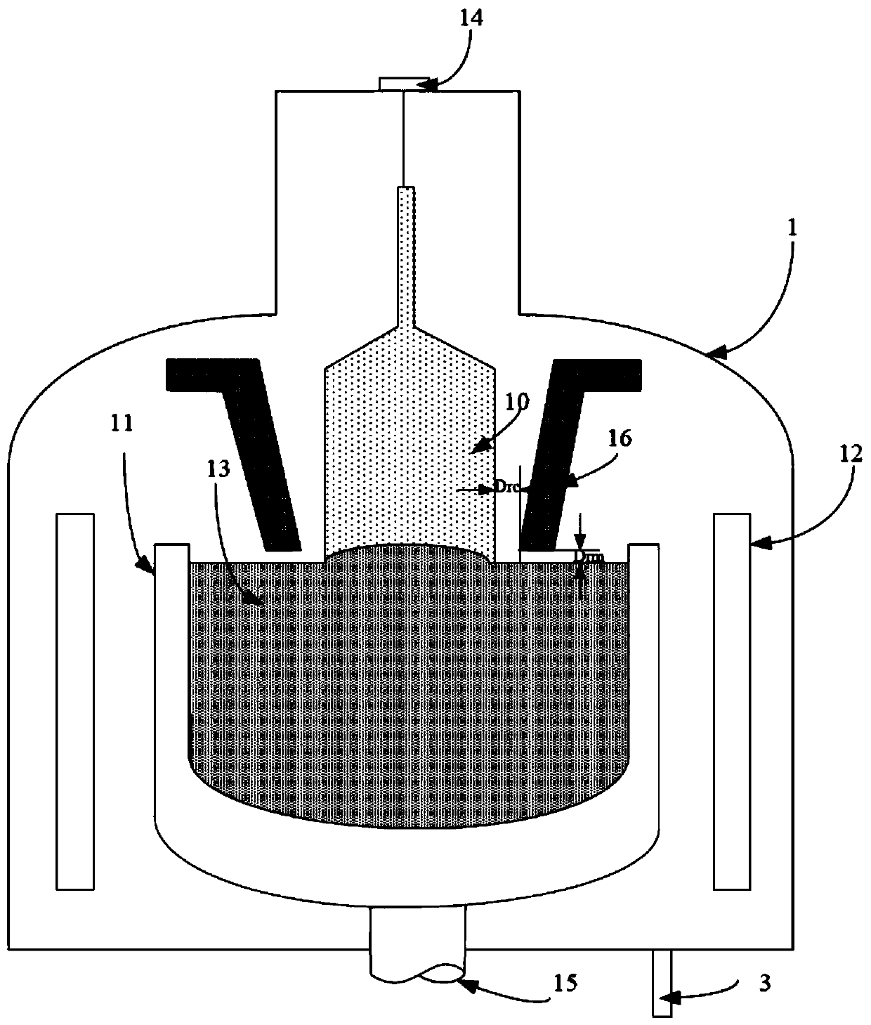
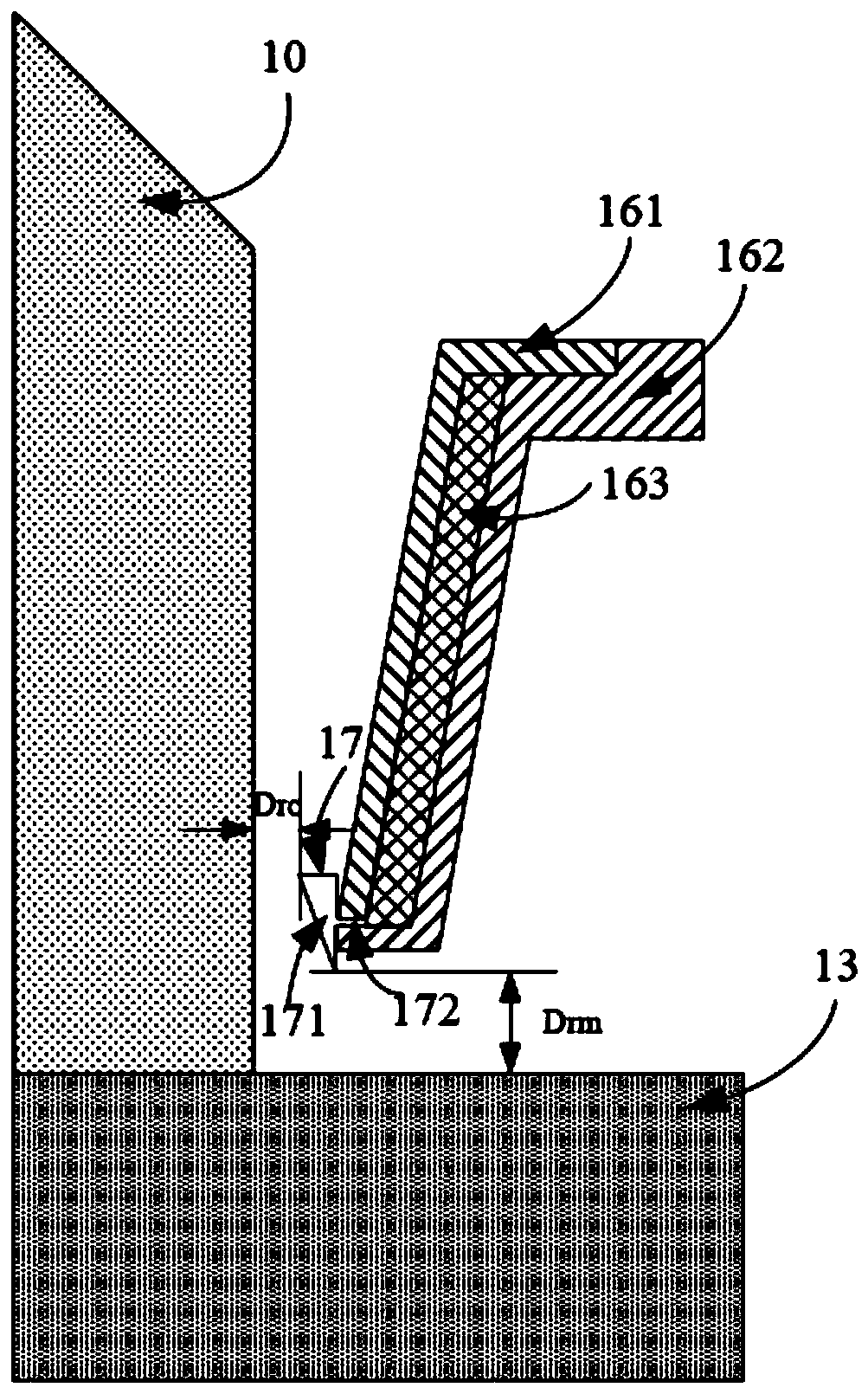
When the heat shield device is fixed, the shape and position of the guide tube are fixed. When the diameter of the silicon crystal rod is constant, it is difficult to further reduce the Drc to achieve a large axial temperature gradient of the silicon crystal. Realization of the control of the screen device itself

Method used


Image

  • Semiconductor crystal growth device
  • Semiconductor crystal growth device
  • Semiconductor crystal growth device

Examples


Embodiment Construction

[0030] In the following description, numerous specific details are given in order to provide a more thorough understanding of the present invention. It will be apparent, however, to one skilled in the art that the present invention may be practiced without one or more of these details. In other examples, some technical features known in the art are not described in order to avoid confusion with the present invention.

[0031] For a thorough understanding of the present invention, a detailed description will be set forth in the following description to illustrate the semiconductor crystal growth apparatus of the present invention. Obviously, the practice of the invention is not limited to specific details familiar to those skilled in the semiconductor arts. Preferred embodiments of the present invention are described in detail below, however, the present invention may have other embodiments besides these detailed descriptions.

[0032] It should be noted that the terms used h...


PUM

PropertyMeasurementUnit
thicknessaaaaaaaaaa

Abstract

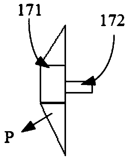
The invention provides a semiconductor crystal growth device. The device comprises a furnace body; a crucible which is arranged in the furnace body and is used for accommodating a silicon melt; a lifting device which is arranged at the top of the furnace body and is used for lifting a silicon crystal bar out of the silicon melt; and a heat shield device which comprises a guide cylinder, wherein the guide cylinder is barrel-shaped and is arranged around the periphery of the silicon crystal bar and is used for rectifying argon inputted from the top of the furnace body and adjusting the distribution of the heat field between the silicon crystal bar and the liquid level of the silicon melt; the heat shield device further comprises an adjusting device arranged on the inner side of the lower endof the flow guide cylinder, and the adjusting device is used for adjusting the minimum distance between the heat shield device and the silicon crystal bar. According to the device, the adjusting device is arranged on the inner side of the lower end of the guide cylinder, the distance between the silicon crystal bar and the heat shield device close to the silicon crystal bar is adjusted without changing the shape and position of the guide cylinder, and the crystal growth speed and quality are improved.

Description

technical field [0001] The invention relates to the field of semiconductor manufacturing, in particular to a semiconductor crystal growth device. Background technique [0002] The Czochralski method (Cz) is an important method for preparing silicon single crystals for semiconductors and solar energy. The high-purity silicon material placed in the crucible is heated to melt it through a thermal field composed of carbon materials, and then the seed crystal is immersed in the In the melt and through a series of processes (seeding, shouldering, equal diameter, finishing, cooling), a single crystal rod is finally obtained. [0003] In the crystal pulling process, a heat shield device, such as a draft tube (or reflective screen), is often provided around the produced silicon crystal rod. On the one hand, it is used to isolate the quartz crucible and the silicon melt in the crucible from the crystal during the crystal growth process. The heat radiation generated on the surface inc...

Claims


Application Information

Patent Timeline
Patent Type & Authority Applications(China)
IPC IPC(8): C30B15/00C30B29/06
CPCC30B15/00C30B29/06C30B15/20C30B15/14Y02P70/50C30B15/007Y10T117/1068
Inventor 沈伟民王刚邓先亮
Owner ZING SEMICON CORP
Why Eureka
Try Eureka