X-ray detector structure and working method thereof

A technology of optical detectors and detector chips, which is applied in the field of X-ray detectors, can solve the problems of unresolved scintillators, absorption, and high quality, and achieve the effects of solving insufficient detection efficiency, improving absorption capacity, and reducing light output

Active Publication Date: 2020-08-11
奕瑞新材料科技(太仓)有限公司
View PDF9 Cites 1 Cited by
  • Summary
  • Abstract
  • Description
  • Claims
  • Application Information

AI Technical Summary

Problems solved by technology

[0005] However, a thicker scintillator will bring some problems: First, as the thickness of the scintillator increases, the visible light absorbed by X-rays needs a longer path to be transmitted to the surface of the detector chip, while the visible light transmission In the process, it may be absorbed
[0007] The Chinese patent application No. CN201910706450.5 discloses an X-ray detector and its preparation method. The first photosensitive layer and the second photosensitive layer arranged on both sides of the scintillator layer are independently coupled and sampled, and the low-radiation Under the single exposure condition of the dose, the spatial resolution and the fluorescence absorption rate are improved at the same time, the radiation dose and the signal-to-noise ratio are optimized, and the problems such as the decrease of the light output caused by the increase of the thickness of the scintillator and the damage caused by the large mass are not solved.

Method used


Image

  • X-ray detector structure and working method thereof
  • X-ray detector structure and working method thereof
  • X-ray detector structure and working method thereof

Examples


Embodiment

[0050] Based on the above structural basis, such as Figure 4-8 shown.

[0051] The working method of the X-ray detector structure of the present invention comprises the following steps:

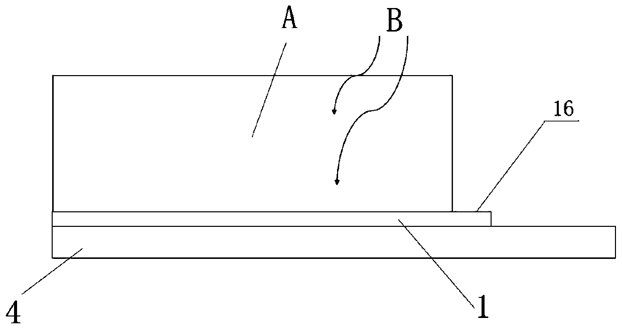
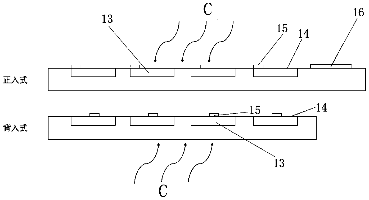
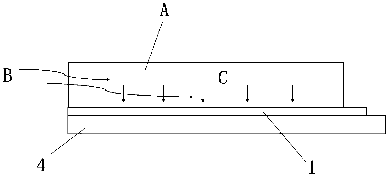
[0052] (1) The incident X-ray B enters the pixels 111 corresponding to the front scintillator 2 and the back scintillator 3, and is respectively absorbed in the respective pixels 111 of the front scintillator 2 and the back scintillator 3 to release visible light;

[0053] (2) After reflection, the visible light C produced by the front scintillator 2 enters the normal incident surface 111 of the detector chip 1 from the light-emitting surface of the front scintillator 2 and is absorbed by the detector chip 1 to form a photogenerated charge a; the back scintillator 3 After being reflected, the produced visible light C is irradiated from the light-emitting surface of the back scintillator 3 into the back incidence surface 12 of the detector chip 1, and is absorbed by the detector to form phot...


PUM


Abstract

The invention discloses an X-ray detector structure and a working method thereof. The X-ray detector structure comprises a detector chip, a front scintillator, a back scintillator, a substrate and a fixing structure, wherein the detector chip comprises a front incident plane and a back incident plane; the photosensitive area of the front incident surface is attached to the front scintillator, andthe photosensitive area of the back incident surface is attached to the back scintillator; the non-photosensitive area of the detector chip is attached to the substrate; and one end or two ends of thedetector chip is / are provided with a signal transmission area which is conducted to the substrate through binding wires. According to the X-ray detector structure and the working method thereof, thestructural design is reasonable, and the working method is simple; a double-sided incidence mode is adopted, so that the thickness of the whole scintillator of the X-ray detector is increased, and meanwhile, the light output of the scintillator is not reduced; and the area of the detector chip is not increased, the signal magnitude is ensured, the imaging quality is improved, and the application prospect is wide.

Description

technical field [0001] The invention relates to the technical field of X-ray detectors, in particular to an X-ray detector structure and a working method thereof. Background technique [0002] An X-ray detector is a device that converts X-ray energy into electrical signals that can be recorded. It is usually composed of a scintillator, a detector chip, and a substrate, such as figure 1 As shown, the working principle is that X photons are incident into the scintillator, converted into visible light output, and enter the detector chip. Then the photoelectric conversion is performed by the detector chip to form an electrical signal, which is transmitted to the subsequent signal processing chip through the wires on the chip and the substrate to form the final image. [0003] According to the direction of the incident light, the detector chip is divided into two types: front entry type and back entry type, such as figure 2 As shown, in the front-type detector chip, the visibl...

Claims


Application Information

Patent Timeline
Patent Type & Authority Applications(China)
IPC IPC(8): G01T1/20
CPCG01T1/2002
Inventor 孙磊刘柱王伟李岩
Owner 奕瑞新材料科技(太仓)有限公司
Why Eureka
Try Eureka