Fingerprint recognition device

A fingerprint identification and oxide technology, which is applied in radiation control devices, character and pattern recognition, and acquisition/organization of fingerprints/palmprints, etc., can solve the problems of large occupied area, achieve low power consumption, high electron mobility, sensitive The effect of recognition effect

Pending Publication Date: 2020-08-11
FUJIAN HUAJIACAI CO LTD
View PDF0 Cites 0 Cited by
  • Summary
  • Abstract
  • Description
  • Claims
  • Application Information

AI Technical Summary

Problems solved by technology

[0004] For this reason, it is necessary to provide a new fingerprint identification device to solve the problem of excessive occupied area of ​​the prior art

Method used


Image

  • Fingerprint recognition device
  • Fingerprint recognition device
  • Fingerprint recognition device

Examples


Embodiment Construction

[0017] In order to explain in detail the technical content, structural features, achieved goals and effects of the technical solution, the following will be described in detail in conjunction with specific embodiments and accompanying drawings.

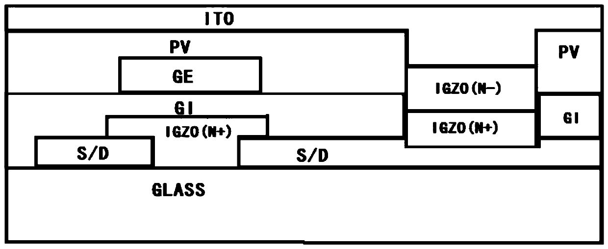
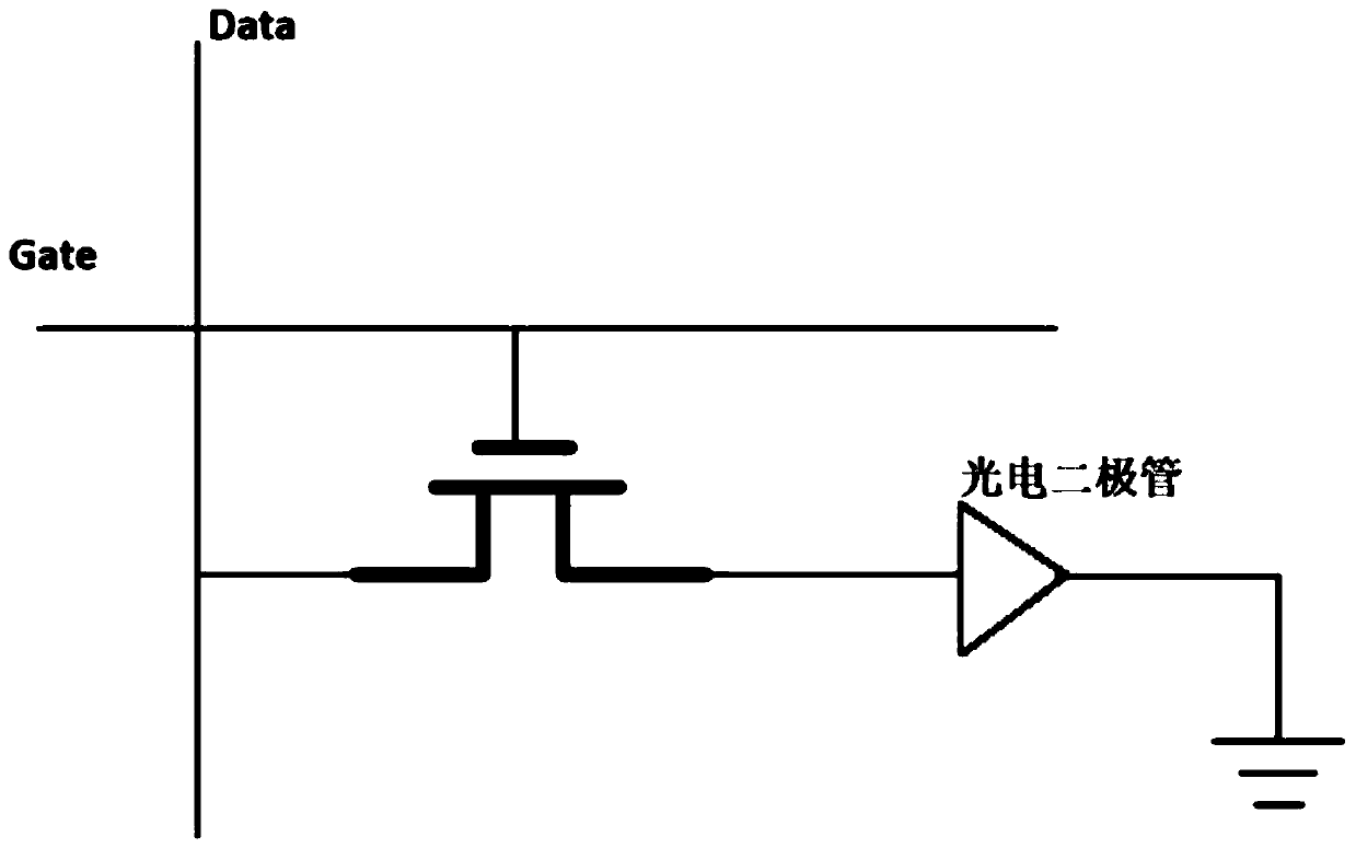
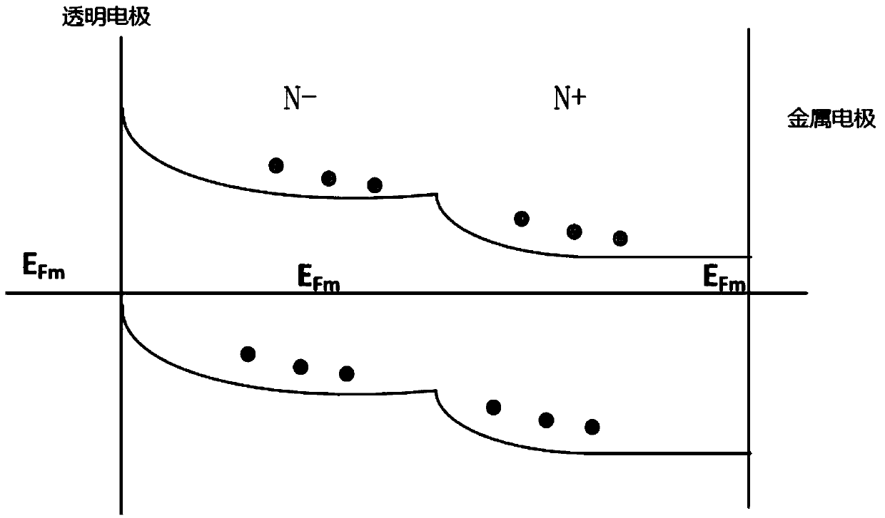
[0018] In some specific examples, see here figure 1 , which is a new type of fingerprint identification device introduced by the present invention, wherein there are several photoelectric sensing modules, including a substrate glass, on which the first electrode SD and the second electrode SD are arranged. figure 1 In the illustrated embodiment, it can be seen that the left side is the source electrode, and the right side is the drain electrode Drain; the active layer N+ is arranged between the first electrode and the second electrode, and the top gate GE is arranged on the active layer. The second electrode is also connected to the oxide electron layer N+, an oxide hole layer N- is arranged on the oxide electron layer, a transparent ...


PUM


Abstract

A fingerprint identification device comprises a substrate, wherein a first electrode and a second electrode are arranged on the substrate, an active layer is arranged between the first electrode and the second electrode, a top gate is arranged on the active layer, the second electrode is further connected with an oxide electronic layer, an oxide hole layer is arranged on the oxide electronic layer, and a transparent oxide layer is arranged on the oxide hole layer. Different from the prior art, the technical scheme designs the photoelectric detection element through designing the transparent oxide layer, and has higher electron mobility, thereby achieving a more sensitive recognition effect and lower power consumption.

Description

technical field [0001] The invention relates to an under-screen fingerprint identification technology, in particular to a fingerprint identification technical solution capable of reducing power consumption. Background technique [0002] The fingerprint recognition under the mobile phone screen is sought after by the market. At present, more and more high-end mobile phones adopt the fingerprint recognition module under the screen. The current mainstream fingerprint design under the screen adopts the optical fingerprint recognition module, and generally uses the photoelectric sensor. [0003] The photoelectric sensing component is composed of a photosensor and a thin film transistor, wherein the photosensor is used to convert the light signal into an electrical signal, and the thin film transistor is used to control the transmission of the electrical signal generated by the photosensor. When using a-Si-based photoelectric sensor components, due to the limitations of a-si mobil...

Claims


Application Information

Patent Timeline
IPC IPC(8): G06K9/00H01L27/146H01L31/0224
CPCH01L31/022475H01L27/1461G06V40/1318
Inventor 刘汉龙刘振东孔藝栋曹尚操郑聪秀
Owner FUJIAN HUAJIACAI CO LTD
Why Eureka
Try Eureka