Radio frequency interface circuit

A radio frequency interface and circuit technology, applied in circuit devices, printed circuits, printed circuit components, etc., can solve the problems of difficult to meet the mounting and drag welding methods, increased insertion loss, large standing wave ratio, etc. Ultra-wideband impedance matching, miniaturization, and the effect of reducing high frequency VSWR and insertion loss

Active Publication Date: 2020-08-14
FENGHUO COMM SCI & TECH CO LTD
View PDF4 Cites 2 Cited by
  • Summary
  • Abstract
  • Description
  • Claims
  • Application Information

AI Technical Summary

Problems solved by technology

[0003] see figure 1 and figure 2 As shown, the most commonly used PCB processing method for the IPEX antenna connector 9 on a single board at present is: two third pads 8 and one second pad 3 are provided on the PCB 1, and the third pad 8 and the second pad The pads 3 are respectively used for mounting and welding the ground pad and the antenna pad of the IPEX antenna connector 9, and the second pad 3 is directly connected to a pin 41 of the DC blocking capacitor through a 50ohm transmission line (usually a microstrip transmission line) 4 ( figure 1 The pad on the right side of pin 41 is another pin of the DC blocking capacitor), simulation and actual tests show that this conventional PCB processing method has some disadvantages: as the operating frequency increases, the VSWR of IPEX antenna connector 9 (Voltage Standing Wave Ratio, standing wave ratio) is on the rise, and the insertion loss will also increase accordingly, especially the problem of large standing wave ratio and large loss in the frequency band above 5GHz, so the transmission of high-frequency signals above 5GHz is harmful to the RF interface circuit. Or the insertion loss and impedance matching of the antenna connector put forward stricter requirements
The standard RF interface circuit form of traditional PCB is difficult to meet the different welding methods of mounting and drag welding

Method used


Image

  • Radio frequency interface circuit
  • Radio frequency interface circuit
  • Radio frequency interface circuit

Examples


Embodiment Construction

[0055] The present invention will be described in further detail below in conjunction with the accompanying drawings and embodiments.

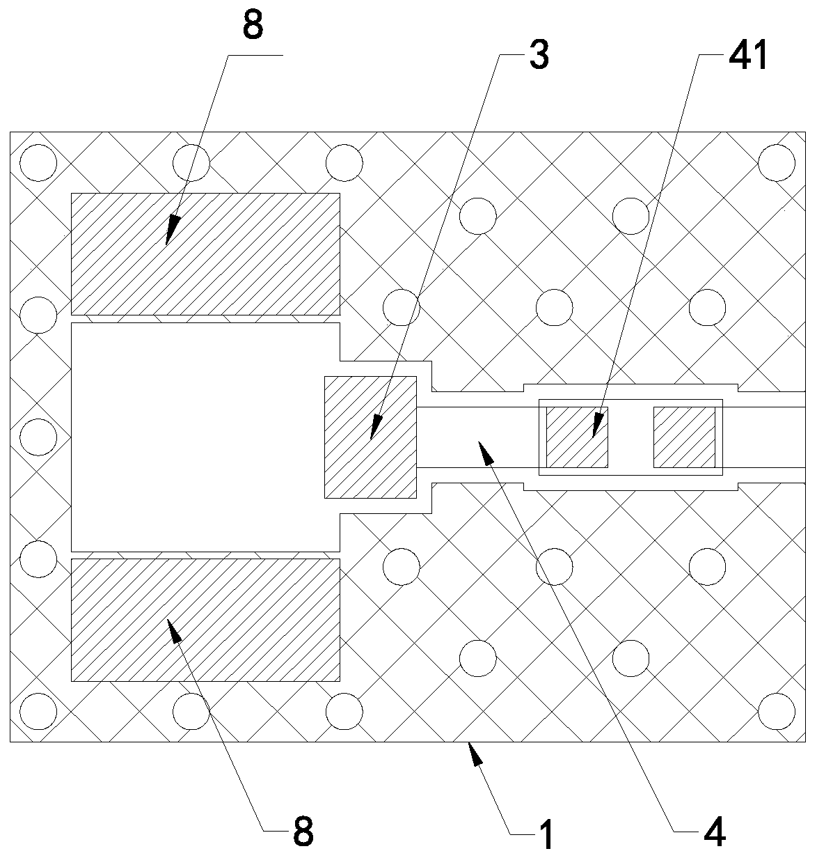
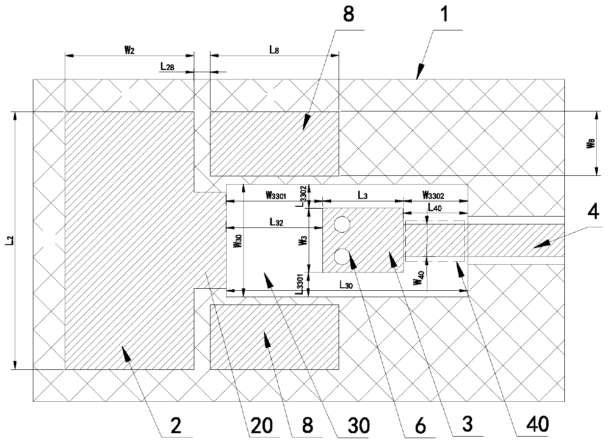
[0056] see Figure 3 to Figure 6 As shown, the first embodiment of the present invention provides a radio frequency interface circuit, which includes a PCB board 1, on the top layer of the PCB board 1, from one end to the other end, there are sequentially provided with a first pad 2, a second pad Disc 3 and transmission line 4, the first pad 2, the second pad 3 are respectively used for dragging the shielding ground net and the core wire of tin welding shielded cable 7, and transmission line 4 usually adopts radio frequency microstrip line; Also set on PCB board 1 There is a first impedance matching network for compensating impedance.

[0057] In the present invention, the top layer and the bottom layer are relative concepts, which refer to the two sides of the PCB board 1. When one of the faces is called the top layer, the other surface oppo...


PUM


Abstract

The invention discloses a radio frequency interface circuit which comprises a PCB, a first bonding pad, a second bonding pad and a transmission line are sequentially arranged on the top layer of the PCB from one end to the other end of the PCB, and the first bonding pad and the second bonding pad are used for dragging tin to weld a shielding ground net and a core wire of a shielding cable respectively; the PCB is also provided with a first impedance matching network used for compensating impedance. The first impedance matching network comprises a matching branch knot and a metallized through hole, the matching branch knot is arranged on the bottom layer of the PCB, a second hollowed-out area is arranged in the periphery of the matching branch knot, the metallized through hole is formed inthe PCB, and the two ends of the metallized through hole are connected with the second bonding pad and the matching branch knot respectively. According to the invention, the inherent impedance discontinuity of the original radio frequency interface circuit and the difference of different frequency bands can be eliminated, and the high-frequency standing-wave ratio and the insertion loss are reduced, so that the ultra-wideband impedance matching is realized.

Description

technical field [0001] The invention relates to the technical field of circuit board design, in particular to a radio frequency interface circuit. Background technique [0002] With the gradual application of WiFi 6 and 5G technology, the frequency of radio frequency (RF) is getting higher and higher, and the RF interface circuit or antenna connector used to connect the antenna to the PCB (Printed Circuit Board, printed circuit board) is extended to Frequency bands above 5 GHz present significant challenges. IPEX (Interconnect and Packaging Electronics, electronic assembly interconnection) antenna connector is used as the interface between the radio frequency interface circuit and the antenna. Due to its small size and low price, it is widely used in WLAN (Wireless Local Area Network, wireless local area network), routers, GPS, mobile phones and other product boards for radio frequency signal transmission. [0003] see figure 1 and figure 2 As shown, the most commonly u...

Claims


Application Information

Patent Timeline
Patent Type & Authority Applications(China)
IPC IPC(8): H05K1/02H01Q1/50
CPCH01Q1/50H05K1/025H05K1/0251
Inventor 张先勇石胜兵万波刘水亮
Owner FENGHUO COMM SCI & TECH CO LTD
Why Eureka
Try Eureka