

Wafer defect detection equipment
A defect detection and wafer technology, applied in the direction of optical defect/defect, image data processing, instrument, etc., can solve the problems of low detection efficiency, low output per unit time, data processing lag, etc., and the time to reach is reduced and reduced Volume, efficiency-enhancing effect
- Summary
- Abstract
- Description
- Claims
- Application Information
AI Technical Summary
Problems solved by technology
Method used
Image

Examples
Embodiment Construction
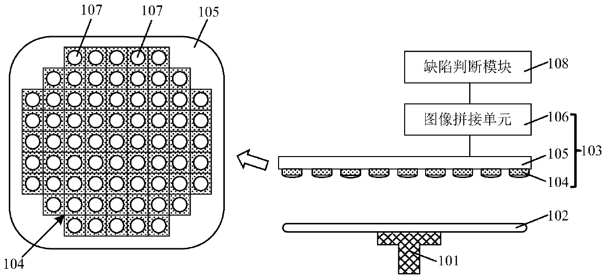
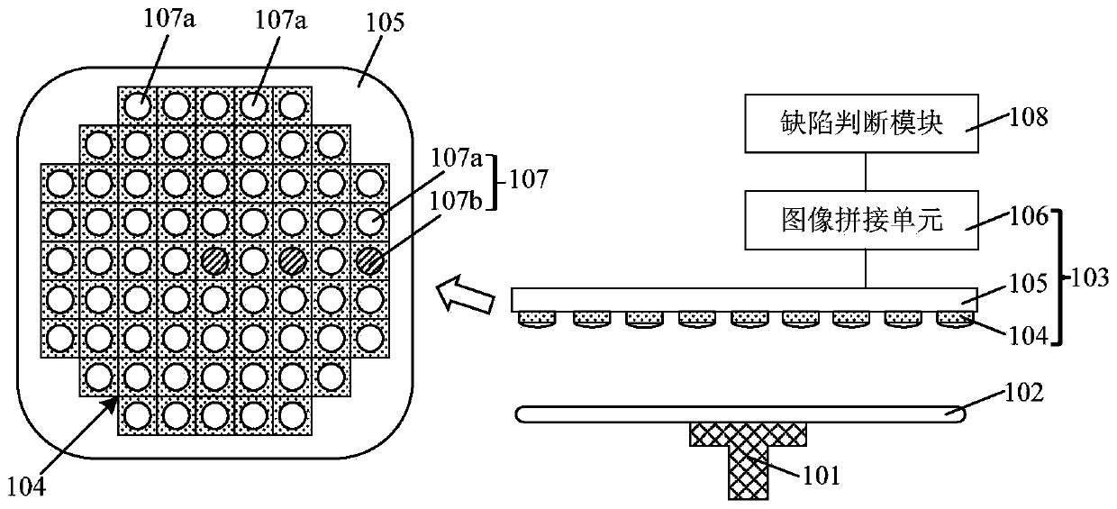
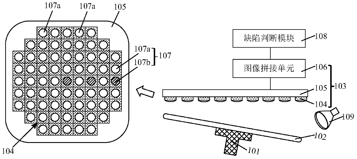
[0031] The invention provides a wafer defect detection device, comprising: a wafer carrier, used to fix the wafer to be detected; an image acquisition module, the image acquisition module includes a camera array, and the image acquisition module takes a single shot through the camera array Obtain a detection image corresponding to the entire surface of the wafer to be detected; a defect judgment module, the defect judgment module judges whether there is a defect on the surface of the wafer to be detected according to the detection image obtained by the image acquisition module. The image acquisition module obtains the inspection image corresponding to the entire surface of the wafer to be inspected by one shot of the camera array, so the wafer stage does not need to scan and move (moving in the horizontal direction) when acquiring the inspection image, and the application The wafer stage described in the above only needs to move in a small range or a small distance in the verti...
PUM
 Abstract
Description
Claims
Application Information