Light emitting diode and manufacturing method thereof

A technology of light-emitting diodes and light-emitting layers, which is applied in the direction of electrical components, circuits, semiconductor devices, etc., can solve the problems of light-emitting efficiency drop, peak efficiency shift, etc., and achieve simplified structure layers, small stress, and reduced piezoelectric polarization effects Effect

Active Publication Date: 2020-08-18
JIANGSU INST OF ADVANCED SEMICON CO LTD
View PDF7 Cites 2 Cited by
  • Summary
  • Abstract
  • Description
  • Claims
  • Application Information

AI Technical Summary

Problems solved by technology

How to avoid the shift of peak efficiency to the non-working area under low current density injection, and at the same time avoid a sharp drop in light extraction efficiency is a problem faced by the existing technology

Method used


Image

  • Light emitting diode and manufacturing method thereof
  • Light emitting diode and manufacturing method thereof
  • Light emitting diode and manufacturing method thereof

Examples


Embodiment Construction

[0020] The specific implementation of the light-emitting diode (LED) and its manufacturing method provided by the present invention will be described in detail below in conjunction with the accompanying drawings.

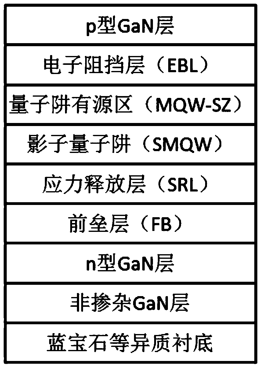
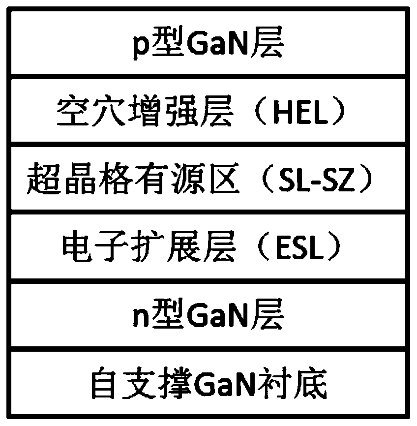
[0021] attached figure 2 Shown is a schematic diagram of the structure of the LED described in this specific embodiment, including a self-supporting substrate layer, and an n-type semiconductor layer, a light-emitting layer, and a p-type semiconductor layer on the surface of the self-supporting substrate, wherein the light-emitting The layers include an electron spreading layer (ESL), a superlattice active zone (SL-SZ), and a hole enhancing layer (HEL).

[0022] In this specific embodiment, the self-supporting substrate is a GaN self-supporting substrate, which can be polar or non-polar. The n-type semiconductor layer, light-emitting layer, and p-type semiconductor layer are sequentially an n-type GaN layer, a light-emitting layer, and a p-type GaN layer, and the ...


PUM

PropertyMeasurementUnit
thicknessaaaaaaaaaa
thicknessaaaaaaaaaa
thicknessaaaaaaaaaa

Abstract

The invention provides a light emitting diode which comprises a self-supporting substrate layer, and an n-type semiconductor layer, a light emitting layer and a p-type semiconductor layer which are arranged on the bottom surface of the self-supporting substrate layer. The light emitting layer comprises an electron expansion layer, a superlattice active region and a hole enhancement layer. According to the structure, the light emitting efficiency under low current density can be improved.

Description

technical field [0001] The invention relates to the field of semiconductor lighting, in particular to a light emitting diode. Background technique [0002] GaN-based light-emitting diodes (LEDs) are widely used because the light-emitting layer can mix narrow-bandgap InGaN materials (corresponding to long-wavelength light) and wide-bandgap AlGaN materials (corresponding to short-wavelength light), thereby achieving full-spectrum light emission. In lighting display and its related applications. attached figure 1 Shown is a schematic diagram of a chip-sized GaN-based LED epitaxial structure in the prior art, which is generally used for chips with a size above 100 microns, and is mainly composed of a substrate, an n-type region, a light-emitting active region and a p-type region. Among them, the light-emitting active region uses the multi-quantum well structure (MQW) of In(Al)GaN. By modulating the In(Al) composition, the wavelength in the entire visible light range can be rea...

Claims


Application Information

Patent Timeline
Patent Type & Authority Applications(China)
IPC IPC(8): H01L33/06H01L33/00H01L33/12H01L33/14H01L33/32
CPCH01L33/0075H01L33/06H01L33/12H01L33/145H01L33/325
Inventor 王国斌王建峰徐科
Owner JIANGSU INST OF ADVANCED SEMICON CO LTD
Why Eureka
Try Eureka