Lower electrode surface dielectric layer and manufacturing process thereof

A surface dielectric layer and electrode surface technology, applied in circuits, discharge tubes, electrical components, etc., can solve the problems of reducing the contact area between the lower electrode and the glass panel, insufficient He gas flow of the cooling gas, and poor heat dissipation of the glass panel. Poor heat dissipation, reduced debris and poor cooling, moderate contact area effect

Pending Publication Date: 2020-08-21
芜湖通潮精密机械股份有限公司
View PDF3 Cites 0 Cited by
  • Summary
  • Abstract
  • Description
  • Claims
  • Application Information

AI Technical Summary

Problems solved by technology

The surface of the flat plate bottom electrode is an extremely dense peak and trough alternate flat structure, the surface roughness is Ra2~6μm, and the contact area with the glass panel is large, which is not easy to cause mura defects on the glass panel. However, due to the large contact area with the glass panel, the glass panel and the bottom The gap between the electrodes is small, resulting in insufficient cooling gas and gas flow between the glass panel and the surface of the lower electrode, which is prone to poor heat dissipation of the glass panel and lower yield. In addition, the large contact area makes it easier for the glass to stick to the surface of the lower electrode. , when the lift pin (thimble) is pushed out of the glass, there will be fragments
Bump type bottom electrode, bump height 20-100μm, bump diameter φ0.4-φ1.2, bump pitch 2-10mm, glass directly contacts with bump surface, reducing the contact area between bottom electrode and glass panel , brings good heat dissipation and solves the debris problem, but the glass is only in contact with the surface bumps, and Mura (uneven display brightness) is prone to appear at the contact position with the glass panel

Method used


Image

  • Lower electrode surface dielectric layer and manufacturing process thereof
  • Lower electrode surface dielectric layer and manufacturing process thereof
  • Lower electrode surface dielectric layer and manufacturing process thereof

Examples


Embodiment Construction

[0032] In the present invention, it should be understood that the terms "length", "width", "upper", "lower", "front", "rear", "left", "right", "vertical", "horizontal" ", "Top", "Bottom", "Inner", "Outer", "Clockwise", "Counterclockwise", "Axial", "Plane Direction", "Circumferential" and other indications are based on The orientation or positional relationship shown in the drawings is only for the convenience of describing the present invention and simplifying the description, and does not indicate or imply that the referred device or element must have a specific orientation, be constructed and operated in a specific orientation, and therefore cannot be understood as Limitations on the Invention.

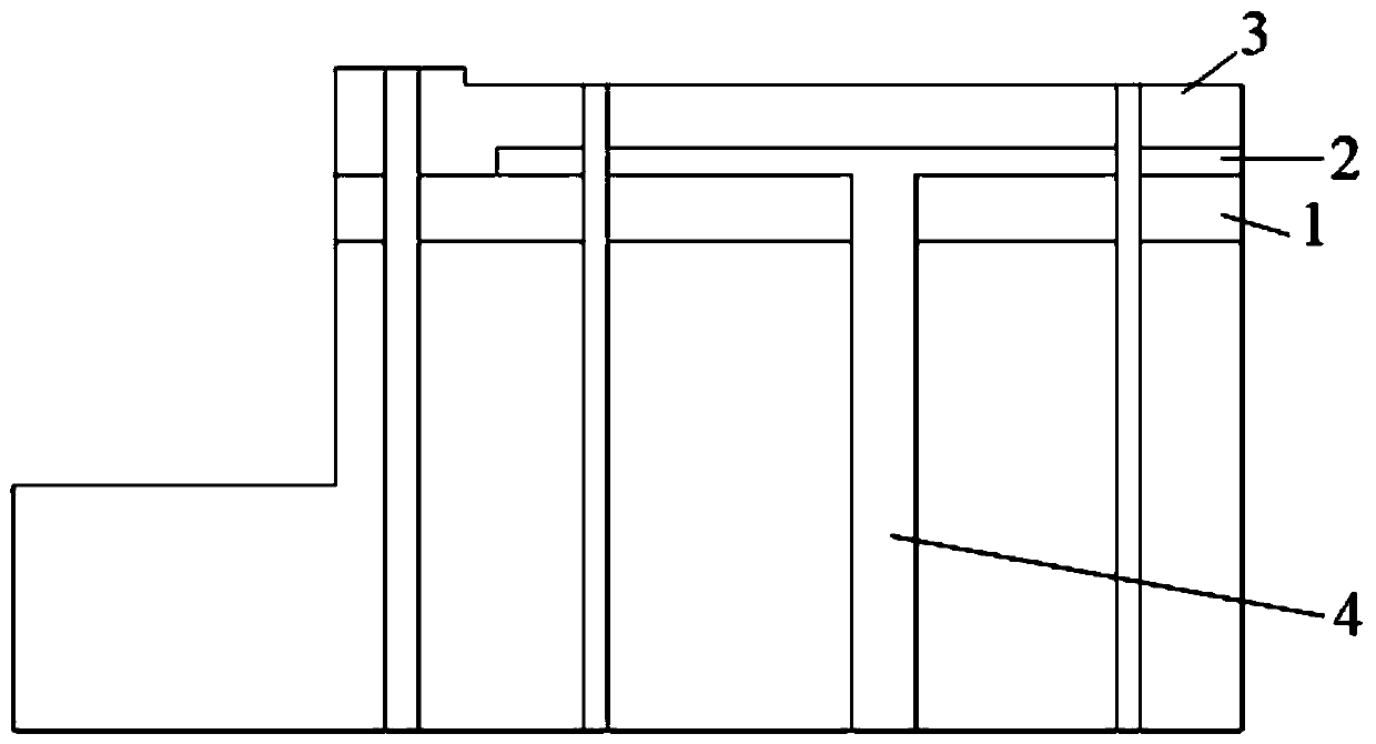
[0033] like figure 1 As shown, a dielectric layer on the surface of the lower electrode, the lower electrode includes a bottom insulating layer 1, a tungsten conductive layer 2, a surface dielectric layer 3 and an electrode column 4, and it is characterized in that: the surface die...


PUM

PropertyMeasurementUnit
Bump heightaaaaaaaaaa
Roughnessaaaaaaaaaa
Pressureaaaaaaaaaa

Abstract

The invention discloses a lower electrode surface dielectric layer. The lower electrode comprises a bottom insulating layer, a tungsten conductive layer, a surface dielectric layer and an electrode column, wherein the surface dielectric layer is of a densely distributed convex point structure, the convex points are square or round with a size of 1-3 [mu]m, the height of the convex points is 10-30[mu]m, the distance between the convex points is 1-3 [mu]m, the tungsten conductive layer is arranged between the bottom insulating layer and the surface dielectric layer, and the electrode column penetrates through the bottom insulating layer to be connected with the tungsten conductive layer. The surface dielectric layer of the invention is of a densely distributed convex point structure, wherein the convex points are in square original shapes or circular shapes of 1-3 [mu]m, the heights of the convex points are 10-30 [mu]m, the distances between the convex points are 1-3 [mu]m, and the sizes of the convex points are smaller than or close to the size of a single pixel point of panel glass. According to the structure, the contact area between the glass panel and the surface of the lower electrode is moderate while the gap between the lower electrode and the glass panel is increased, so that the problems of fragments, poor cooling and the like are effectively reduced while the problemthat Mura is likely to occur in a common convex point type is solved through the similar flat plate type outline, and the product quality and yield can be effectively improved.

Description

technical field [0001] The invention belongs to the technical field of lower electrodes, and in particular relates to a dielectric layer on the surface of a lower electrode and a manufacturing process thereof. Background technique [0002] The dry etching machine is the key equipment in the process of liquid crystal panel and semiconductor preparation. The lower electrode is the key component in the dry etching machine. The lower electrode is a typical sandwich structure, which is composed of the bottom insulating layer, the tungsten conductive layer and the surface dielectric layer. When the etching machine is working, the glass substrate is placed on the surface of the lower electrode, which is in direct contact with the dielectric layer of the lower electrode. The DC power supply is connected to the tungsten conductive layer through the DC electrode column on the back of the lower electrode to make it negatively charged, and the lower surface of the glass generates an indu...

Claims


Application Information

Patent Timeline
IPC IPC(8): H01J37/32
CPCH01J37/32532H01J37/32541H01J2237/334
Inventor 何新玉赵浩司奇峰
Owner 芜湖通潮精密机械股份有限公司
Why Eureka
Try Eureka