

ESD circuit capable of improving high-voltage reliability
A reliability and circuit technology, applied in the field of ESD circuits, can solve the problems of large chip area, high complexity, and low reliability of high-voltage resistance, etc., and achieve the goal of reducing chip area, reducing complexity, and reducing connection complexity Effect
- Summary
- Abstract
- Description
- Claims
- Application Information
AI Technical Summary
Problems solved by technology
Method used
Image

Examples
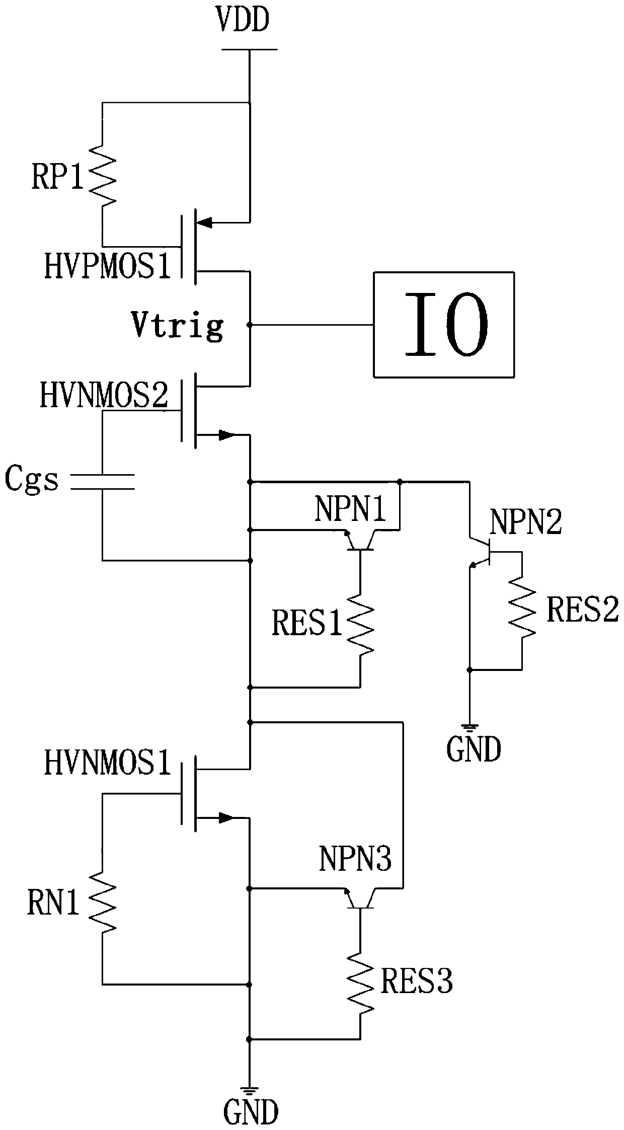
Embodiment 1
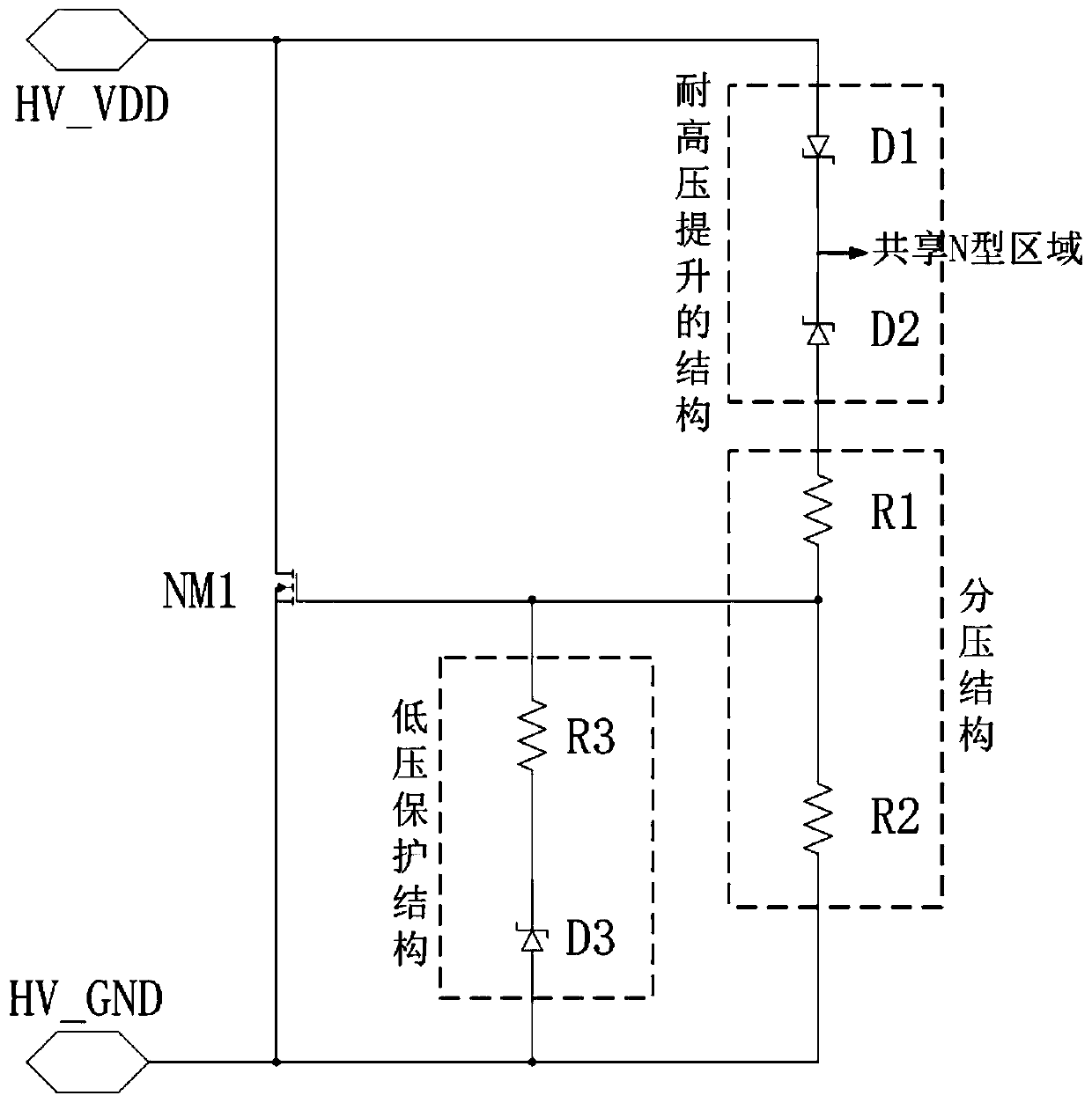
[0036] refer to figure 2 , the present invention provides an ESD circuit for improving high-voltage reliability, including a DC high-voltage-resistant power supply ESD input terminal, a DC high-voltage-resistant ground input terminal, a high-voltage-resistant boost structure, a voltage dividing structure, a low-voltage protection structure, and a high-power NMOS tube .
[0037] In this embodiment, the high-voltage boosting structure is composed of a high-voltage forward-conducting high-voltage diode D1 and a high-voltage reverse-conducting high-voltage diode D2. When the breakdown voltage and the forward conduction voltage drop of the high voltage diode D1, this structure is turned on; adjust the series high voltage diode D1, this structure can increase the reverse breakdown voltage of the high voltage diode D2; the series high voltage diode D1 can also increase the reverse conduction high voltage The high-voltage reliability of the diode D2; this structure can share the N-t...
PUM
 Abstract
Description
Claims
Application Information