Semiconductor device and manufacturing method thereof

A manufacturing method and semiconductor technology, applied in semiconductor/solid-state device manufacturing, semiconductor devices, electrical components, etc., can solve problems such as uneven distribution of impurities in the P-well region, different turn-on voltage, and affecting the electrical characteristics of the device, so as to achieve optimal electrical properties. Characteristics and reliability, optimized uniformity, effects of reducing adverse defects

Pending Publication Date: 2020-08-25
JOULWATT TECH INC LTD
View PDF7 Cites 2 Cited by
  • Summary
  • Abstract
  • Description
  • Claims
  • Application Information

AI Technical Summary

Problems solved by technology

[0003] However, since the P well region of the traditional structure is formed by implantation, in the semiconductor body region, the distribution of impurities in the P well region in the vertical direction is not uniform.
It will lead to different turn-on voltages of channel regions with different depths on the sidewall of the groove gate, corresponding to different threshold voltages, and affecting the electrical characteristics of the device

Method used


Image

  • Semiconductor device and manufacturing method thereof
  • Semiconductor device and manufacturing method thereof
  • Semiconductor device and manufacturing method thereof

Examples


Embodiment Construction

[0031] Various embodiments of the invention will be described in more detail below with reference to the accompanying drawings. In the various drawings, the same elements are denoted by the same or similar reference numerals. For the sake of clarity, various parts in the drawings have not been drawn to scale.

[0032] The specific implementation manners of the present invention will be further described in detail below in conjunction with the accompanying drawings and embodiments.

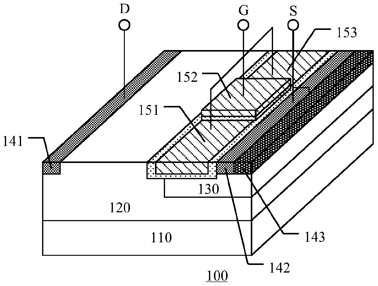
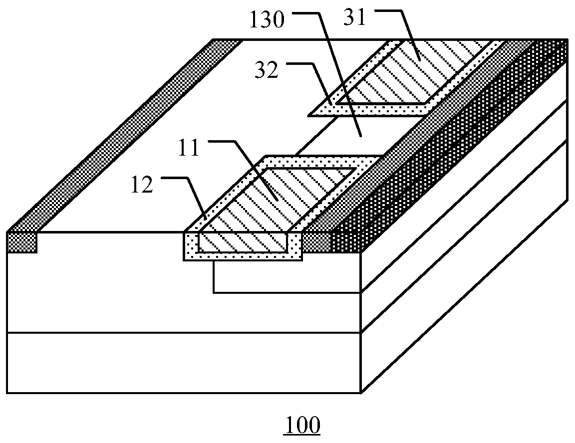
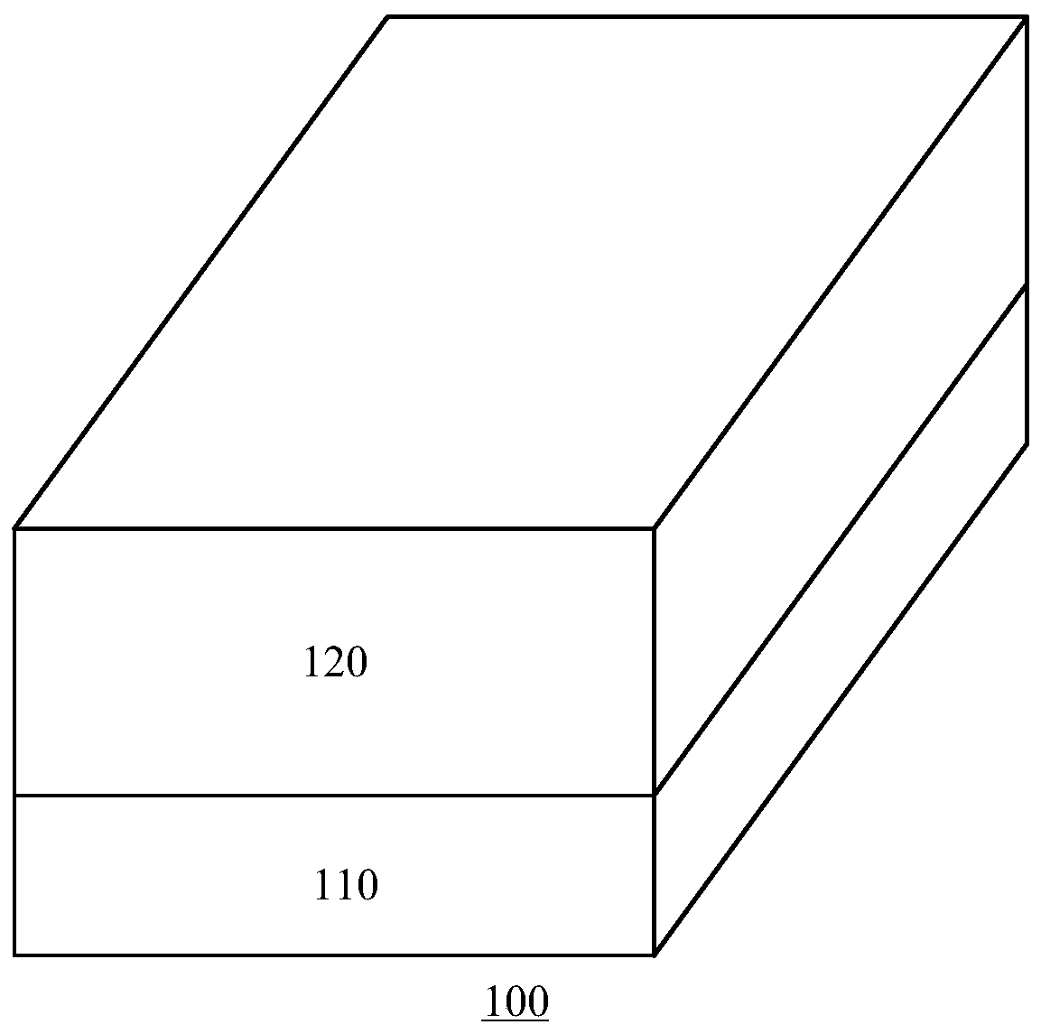
[0033] figure 1 shows a schematic structural diagram of a tri-gate LDMOS device according to the prior art, figure 2 shows the basis figure 1 A partial structural schematic diagram of the tri-gate LDMOS device. combine figure 1 and figure 2 , a triple-gate LDMOS device 100 in the prior art includes a P substrate 110, an N drift region 120, a P well region 130, an N+ doped region 141, an N+ doped region 142, a P+ doped region 143, a first gate region 151 , the second gate region 152 and the...


PUM


Abstract

The invention discloses a semiconductor device and a manufacturing method thereof. The manufacturing method comprises the steps: forming a drift region on a substrate, and etching a well region trench; obtaining a well region in the well region trench through an epitaxial method; and manufacturing a trench gate structure, a source region and a drain region. According to the semiconductor device and the manufacturing method thereof, the well region is manufactured through etching in an epitaxial mode, so that a well region with uniform doping concentration in the longitudinal direction can be obtained, and the semiconductor device with uniform threshold voltage of a trench gate and a plane gate is obtained. The method is mainly characterized in that the well region is manufactured in an epitaxial mode, the uniformity of the longitudinal doping concentration of the well region is mainly optimized to ensure the consistency of the threshold voltage of the trench gate, so that the electrical property of the device is improved. According to the invention, the advantages of the trench gate can be exerted, and the problem of inconsistent threshold voltages of different parts of the trenchgate can be effectively avoided.

Description

technical field [0001] The invention relates to the technical field of semiconductors, in particular to a semiconductor device and a manufacturing method thereof. Background technique [0002] In order to improve the electrical characteristics of power LDMOS (Laterally Diffused Metal Oxide Semiconductor, Laterally Diffused Metal Oxide Semiconductor), it is usually necessary to increase its BV (Balanced Voltage, balanced voltage) and reduce its specific on-resistance. Common technologies include super junction technology, resurf (Reduced SUR face Field, reduced surface electric field) technology, and slot gate technology. Tri-gate LDMOS is also one of the trench gate technology methods that can effectively reduce the specific on-resistance of devices. It can significantly increase the channel area and reduce the channel resistance, thereby reducing the on-resistance and improving the electrical characteristics of the device. [0003] However, since the P-well region of the ...

Claims


Application Information

Patent Timeline
Patent Type & Authority Applications(China)
IPC IPC(8): H01L29/78H01L21/336H01L29/06H01L29/423
CPCH01L29/7816H01L29/66681H01L29/0603H01L29/0684H01L29/4236
Inventor 葛薇薇
Owner JOULWATT TECH INC LTD
Why Eureka
Try Eureka