Efficient automatic soldering process for patch common-mode inductors

A common mode inductor and patch technology, applied in the field of high-efficiency automated soldering process, can solve problems such as low efficiency, inability to guarantee quantitative control of flux, and unstable quality.

Pending Publication Date: 2020-09-01
苏州恊合自动化科技有限公司
View PDF10 Cites 0 Cited by
  • Summary
  • Abstract
  • Description
  • Claims
  • Application Information

AI Technical Summary

Problems solved by technology

Because the distance between the ACM solder PIN and the coil of the chip common mode inductor is very close, using the traditional manual electric soldering iron soldering process will cause fatal problems such as coil melting, tin tip, patch surface melting tin, false soldering, and uneven solder filling. Satisfy the solder quality requirements, other solder processes cannot solve the above problems
At present, the production process adopts manual brushing of flux, manual electric soldering iron solde

Method used


Image

  • Efficient automatic soldering process for patch common-mode inductors
  • Efficient automatic soldering process for patch common-mode inductors

Examples


Embodiment 1

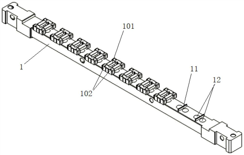
[0030] Please refer to Figure 1-Figure 2 , the present embodiment is a high-efficiency automated soldering process for chip common mode inductors, which includes the following steps:

[0031] 1) A jig bar 1 is provided, and the patch common-mode inductors 101 are placed on the jig bar 1 at intervals. The upper surface of the jig bar 1 is provided with a limiting protrusion inserted into the inside of the patch common-mode inductor 101 for positioning. Lifting 11, the adsorption magnetic block 12 located on both sides of the limit protrusion 11 and adsorbing the patch common mode inductor 101;

[0032] 2) Move the chip common mode inductor 101 loaded with the automatic conveying device to the flux spraying station; the automatic conveying device may be a linear conveying mechanism or a disc rotating conveying mechanism;

[0033] 3) The jig bar 1 is deflected clockwise around a horizontal line to set the angle, and the chip common mode inductor 101 arranged on the jig bar 1 is...


PUM


Abstract

The invention discloses an efficient automatic soldering process for patch common-mode inductors. The process comprises the following steps that (1) patch common-mode inductors are placed on a jig strip at interval, wherein the upper surface of the jig strip is provided with limiting protrusions inserted into the patch common-mode inductors for positioning and adsorption magnetic blocks located onthe two sides of the limiting protrusions and adsorbing the patch common-mode inductor; (2) the jig strip is biased to a set angle, so that the surface of the welding feet PIN on one sides of the patch common-mode inductors is exposed upwards; (3) flux spraying is performed on the exposed surfaces of the welding feet PIN on the side by using precision spraying equipment; (4) the step 2 and the step 3 are repeated, flux spraying of the welding feet PIN on the other side is completed, and then the jig strip is restored to an initial state; (5) hot air is blown; (6) selective wave crest weldingis carried out; (7) cleaning is carried out; and (8) CCD detection is carried out. According to the process, automatic soldering operation can be realized, the soldering efficiency, the soldering precision and the soldering effect are greatly improved.

Description

【Technical field】 [0001] The invention belongs to the technical field of soldering process for inductance elements, in particular to a high-efficiency automatic soldering process for patch common-mode inductors. 【Background technique】 [0002] SMD common mode inductor ACM has the characteristics of small footprint on the circuit board, convenient mass processing and production, and high wiring density. It is widely used in switching power supplies, automotive electronics, security fields, consumer electronics, communication equipment, industrial control and other industries. [0003] During the production process of the chip common mode inductor ACM, the pins on both sides of the chip need to be dipped and soldered. Before welding, a layer of flux needs to be applied, and the pins of the chip common mode inductor ACM are exposed Both the upper surface and the side surface need to be coated with flux. Because the distance between the ACM solder PIN and the coil of the chip c...

Claims


Application Information

Patent Timeline
IPC IPC(8): B23K3/08H05K3/34B23K101/42
CPCB23K3/082B23K3/087B23K3/08H05K3/34B23K2101/42
Inventor 徐光伟梅秋雄李艳杰
Owner 苏州恊合自动化科技有限公司
Why Eureka
Try Eureka