Automatic wafer feeding device for wafer feeding machine

A technology of automatic feeding and driving device, applied in conveyor objects, transportation and packaging, electrical components, etc., can solve the problems of low work efficiency, easy to scratch wafers, affecting the quality of wafers, etc., to improve feeding efficiency , The adjustment operation is simple and convenient, and the wafer quality and pass rate are not affected.

Active Publication Date: 2020-09-04
SHANDONG NOVOSHINE OPTOELECTRONICS CO LTD
View PDF6 Cites 6 Cited by
  • Summary
  • Abstract
  • Description
  • Claims
  • Application Information

AI Technical Summary

Problems solved by technology

[0005] Specifically, the technical problem to be solved by the present invention is to provide an automatic wafer loading device for a loading machine to solve the problem of labor-intensive, low-efficiency, and easy-to-scratch wafers manually placed in the tray. Wafers, technical issues affecting wafer quality

Method used


Image

  • Automatic wafer feeding device for wafer feeding machine
  • Automatic wafer feeding device for wafer feeding machine
  • Automatic wafer feeding device for wafer feeding machine

Examples


Embodiment Construction

[0058] The present invention will be further described below in conjunction with specific examples. However, the uses and purposes of these exemplary embodiments are only used to illustrate the present invention, and do not constitute any form of limitation to the actual protection scope of the present invention, nor limit the protection scope of the present invention thereto.

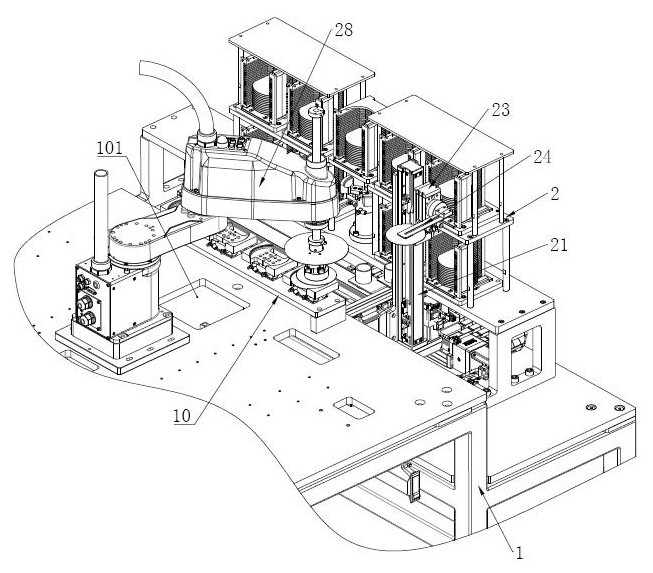
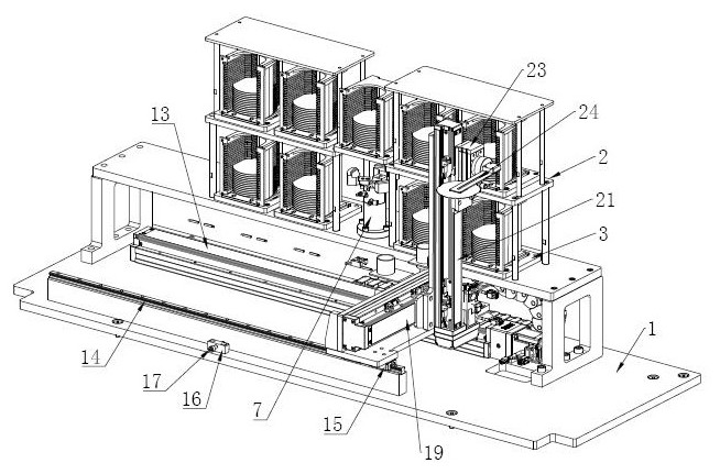
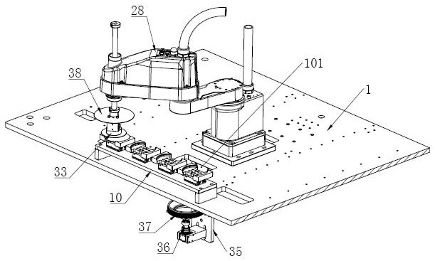
[0059] Such as Figure 1 to Figure 3 As shown, this embodiment provides an automatic wafer loading device for a chip loader, including a frame 1, a material rack 2 for placing flower baskets, a first positioning mechanism and a second positioning mechanism for realizing wafer positioning. Two positioning mechanisms, a turning mechanism for picking up and flipping wafers, and a loading robot arm 28 for realizing wafer loading.

[0060] The material rack 2 is fixedly installed on the frame 1, and the material rack 2 is provided with a number of flower basket mounting plates 3, and the flower basket moun...


PUM


Abstract

The invention belongs to the technical field of wafer loading, and provides an automatic wafer loading device for a wafer loading machine. The device comprises a rack, a material frame, a first positioning mechanism, a second positioning mechanism, a wafer overturning mechanism and a tray loading mechanical arm. The material frame is fixedly installed on the machine frame, the first positioning mechanism is installed on the material frame, a positioning table is further fixedly installed on the machine frame, and the multiple second positioning mechanisms are arranged on the positioning table.The wafer overturning mechanism is located between the material frame and the positioning table and comprises a rotary air cylinder driven by a driving device, a wafer taking plate is fixedly installed on a rotary disc of the rotary air cylinder, and a wafer suction hole is formed in one side of the end of the wafer taking plate. The tray loading mechanical arm is fixedly installed on the machineframe, a wafer taking and placing mechanism is arranged at the executing end of the tray loading mechanical arm, and the machine frame is further provided with a film shooting hole and a shooting mechanism corresponding to the film shooting hole. The feeding efficiency is greatly improved, the wafers cannot be damaged in the feeding process, and it is ensured that the wafer quality and the percent of pass are not affected in the wafer feeding process.

Description

technical field [0001] The invention relates to the technical field of wafer loading, in particular to an automatic wafer loading device for a wafer loading machine. Background technique [0002] Wafer refers to the silicon wafer used to make silicon semiconductor integrated circuits. Because of its circular shape, it is called a wafer. In the process of wafer production and processing, according to the requirements of the processing technology, ICP etching processing of the wafer is required. Before the ICP etching process, the wafers usually need to be arranged and placed in the tray. This process is called wafer loading. , so that during the etching process, the entire tray carrying the wafer is put into the plasma etching machine for etching process. [0003] The produced wafers are divided into front and back. During wafer processing, you should avoid touching the front of the wafer. Touching the front of the wafer will cause contamination or scratches on the wafer, wh...

Claims


Application Information

Patent Timeline
Patent Type & Authority Applications(China)
IPC IPC(8): H01L21/677H01L21/67H01L21/673H01L21/68
CPCH01L21/67259H01L21/67265H01L21/673H01L21/67706H01L21/68
Inventor 李凯杰赵成浩郭明灿王子龙臧运凤
Owner SHANDONG NOVOSHINE OPTOELECTRONICS CO LTD
Why Eureka
Try Eureka