monocrystalline silicon wafer clamping device for reducing TTV and cutting method

A single crystal silicon wafer and clamping device technology, which is applied to fine working devices, manufacturing tools, stone processing equipment, etc., can solve the problems of inability to effectively control TTV and uneven thickness of single crystal silicon wafers, and achieve effective control, Avoid the effect of cutting thickness

Active Publication Date: 2020-09-08
江苏美科太阳能科技股份有限公司
View PDF9 Cites 0 Cited by
  • Summary
  • Abstract
  • Description
  • Claims
  • Application Information

AI Technical Summary

Problems solved by technology

As the use time increases, because the silicon ingot’s cutting surface is completely in contact with the cutting wire net, the hardness of the silicon ingot is high, and the clamping guide rail gasket and metal pad are deformed and worn. Due to the wear of the clamping guide rail and metal pad The position cannot be accurately determined, so there will be different inclination angles in different states. For example, the left side of the silicon in...

Method used


Image

  • monocrystalline silicon wafer clamping device for reducing TTV and cutting method
  • monocrystalline silicon wafer clamping device for reducing TTV and cutting method
  • monocrystalline silicon wafer clamping device for reducing TTV and cutting method

Examples


Embodiment Construction

[0027] The present invention will be described in more detail below with reference to schematic diagrams, wherein preferred embodiments of the present invention are shown, and it should be understood that those skilled in the art can modify the present invention described herein while still achieving the advantageous effects of the present invention. Therefore, the following description should be understood as the broad knowledge of those skilled in the art, but not as a limitation of the present invention.

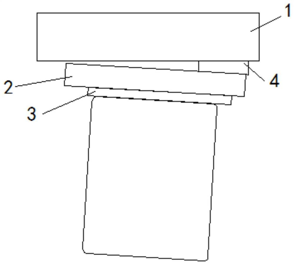
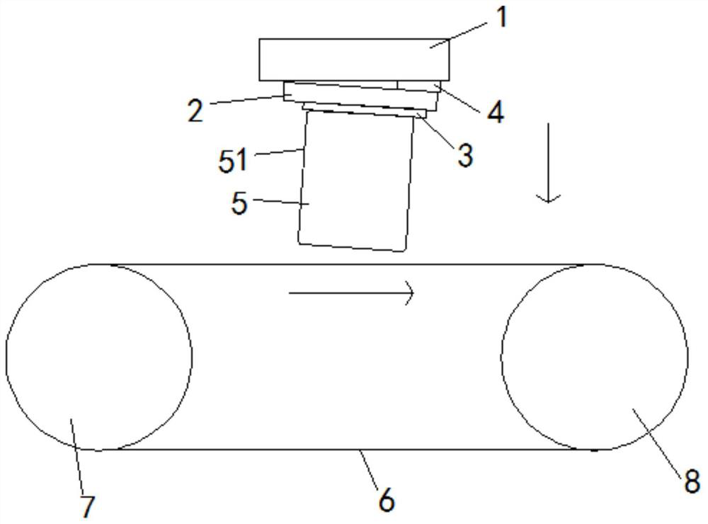
[0028] Such as figure 1 As shown, a clamping device applied to monocrystalline silicon wafers for lowering TTV, including: the first spacer 1, the second spacer 2 and the bonding plate 3 connected in sequence; the first spacer 1 and the second spacer Adjusting shims 4 are arranged between the bars 2.

[0029] The first spacer 1 is fixed and arranged parallel to the running direction of the diamond wire cutting wire mesh 6 . Routing methods include such as figure 1 show...


PUM

PropertyMeasurementUnit
Thicknessaaaaaaaaaa
Line speedaaaaaaaaaa
Wire diameteraaaaaaaaaa

Abstract

The invention provides a monocrystalline silicon wafer clamping device for reducing TTV and a cutting method. The monocrystalline silicon wafer clamping device comprises a first filler strip, a secondfiller strip and a bonding plate which are sequentially connected, wherein the first filler strip is fixed and parallel to the routing direction of a stainless wire cutting wire net, the second filler strip is obliquely arranged, one end of the second filler strip is fixed on the first filler strip, the other end is far away from the first filler strip to form a installing space, an adjusting gasket is arranged in the installing space, one side of the adjusting gasket is fixed on the first filler strip, the other side of the adjusting gasket is fixed on the second filler strip, the bonding plate is parallel to the second gasket, and a silicon ingot is fixed to the side face, away from the second filler strip, of the bonding plate. According to the monocrystalline silicon wafer clamping device in the cutting method, a contact mode between the silicon ingot and the cutting wire net is adjusted from surface contact to point contact, so that the slipping phenomenon when the stainless wireis cut in is avoided, by setting the corresponding relation between the stainless wire feeding direction of the first step of routing and the inclination direction of the silicon ingot during forwardrouting is set, the TTV is effectively controlled.

Description

technical field [0001] The invention belongs to the field of cutting silicon wafers, and in particular relates to a clamping device and a cutting method for monocrystalline silicon wafers for reducing TTV. Background technique [0002] Diamond wire rapidly replaced the traditional cutting method and became the mainstream cutting tool for monocrystalline silicon wafers, and its demand continued to grow as the market share of monocrystalline silicon increased. So far, diamond wire has been widely used in monocrystalline silicon slices around the world. With the promotion of thinner wires, the difficulty of cutting mainly lies in the control of TTV. The silicon ingot clamping device in the prior art includes clamping rail gaskets, metal pads and plastic bonding plates connected in sequence, and the clamping rail pads The sheet is installed on the workbench through the cylinder clamping device. As the use time increases, because the silicon ingot’s cutting surface is completel...

Claims


Application Information

Patent Timeline
IPC IPC(8): B28D5/04B28D7/04
CPCB28D5/045B28D5/0088
Inventor 钱鑫王艺澄
Owner 江苏美科太阳能科技股份有限公司
Why Eureka
Try Eureka