Physical layer transmission real error code acquisition device and equipment

A technology of acquisition device and physical layer, which is applied in the field of real error code acquisition device and equipment for transmission of physical layer, and can solve problems such as inability to guarantee reliable transmission.

Active Publication Date: 2020-09-11
NAT UNIV OF DEFENSE TECH
View PDF5 Cites 0 Cited by
  • Summary
  • Abstract
  • Description
  • Claims
  • Application Information

AI Technical Summary

Problems solved by technology

[0005] The technical problem to be solved by the present invention: aiming at the above-mentioned problems of the prior art, in order to analyze the real bit error characteristics on the physical link under the high-speed serial transmission scene, provide A device and device for collecting actual code errors in physical layer transmission. The invention can realize real-time collection and analysis of physical layer trans

Method used


Image

  • Physical layer transmission real error code acquisition device and equipment
  • Physical layer transmission real error code acquisition device and equipment
  • Physical layer transmission real error code acquisition device and equipment

Examples


Embodiment 1

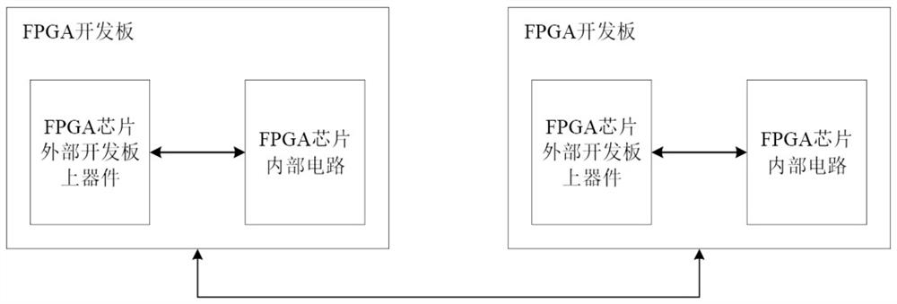
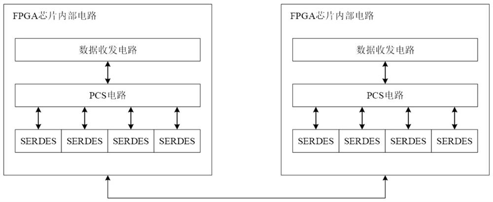
[0032] The real bit error acquisition device for physical layer transmission of the present invention will be further described in detail below by taking the real bit error acquisition device for physical layer transmission implemented in the FPGA development version as a specific example. It should be noted that the carrier of the physical layer transmission real bit error acquisition device of the present invention is not limited to the FPGA chip, and can also be used in other types of processing chips. like figure 1 As shown, the physical layer transmission real error bit acquisition device in this embodiment uses two FPGA development boards with high-speed serial communication interfaces as carriers, and the bottom layer uses optical fibers to connect them, and data is transmitted between the two FPGA development boards. To transmit and collect its error code, each FPGA development board contains the internal circuits of the FPGA chip and the devices on the external develo...

Embodiment 2

[0050] In the aforementioned first embodiment, the transmission data generation circuit generates pseudo-random data through a PRBS random number generator. However, considering that in some test scenarios it is necessary to test the bit error rate of specific data passing through the physical link, a function of testing specific data is added on the basis of Embodiment 1.

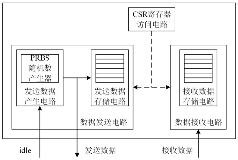
[0051] like Figure 4As shown, the data transmission circuit includes a transmission data generation circuit and a transmission data storage circuit, and the transmission data generation circuit includes a random number generator, a mode configurable data generator and an output selector, a random number generator, a mode configurable data generator They are respectively connected to the input end of the output selector, and the output end of the output selector is connected to the physical coding sublayer circuit PCS. The mode configurable data generator is used to generate specified mode data according t...

Embodiment 3

[0056] In the first and second embodiments above, the physical layer transmission real bit error collection device at the sending end and the physical layer transmission real bit error collection device at the receiving end respectively use their own storage circuits to store the sent data and the received data. However, inside the FPGA chip, the resources of the Block RAM are limited. When the link rate is relatively high, the storage resources of the Block RAM in the FPGA chip will be consumed quickly, resulting in short test time and low test data. Not much. For example, the FPGA chip we usually use has an internal Block RAM with a capacity of about 1000*32Kb, that is, it can store about 120*1024 pieces of 256b data. Under the bandwidth of 4 lanes*2.5Gbps, only about 122880 pieces of 256 data can be sent, and the duration is 3ms. If the consumption of the memory can be reduced, a larger amount of data can be sent and the test time can be increased. Therefore, in order to ...


PUM


Abstract

The invention discloses a physical layer transmission real error code collection device and equipment, and the device comprises an error code rate detection circuit and a data receiving and transmitting circuit connected with a physical coding sub-layer circuit PCS, and the data receiving and transmitting circuit comprises a CSR register access circuit, a data transmitting circuit, and a data receiving circuit. The CSR register access circuit is respectively connected with the data sending circuit and the data receiving circuit, the CSR register access circuit is further connected with an out-of-band access interface, and the data receiving circuit is provided with an output interface used for outputting stored data so as to detect the bit error rate of the data. According to the invention, a physical layer transmission error code can be collected and analyzed in real time when data is transmitted on a high-speed serial link; therefore, the data sent by the sender and the data receivedby the receiver can be analyzed to detect the bit error rate passing through the physical link, and the obtained distribution characteristics and rules of the bit error rate can lay a foundation forthe design of a link fault-tolerant function when the physical link cannot ensure reliable transmission.

Description

technical field [0001] The invention relates to high-speed serial digital communication technology, in particular to a device and equipment for collecting real error codes in physical layer transmission. Background technique [0002] In high-speed digital communication, the traditional parallel transmission method can no longer meet the demand of the increasing communication rate, and the high-speed serial transmission method emerges accordingly. In the serial communication mode, digital communication between nodes is carried out between two adjacent nodes through high-speed serial differential signals. In high-speed serial communication, the user data at the sending end is encoded by the Physical Coding Sublayer (PCS), sent to the high-speed serial-to-parallel converter (SERDES), and converted to serial in SERDES to form a high-speed differential Signal, and then transmit the signal to the opposite end of the link through a pair of high-speed serial differential lines; the...

Claims


Application Information

Patent Timeline
IPC IPC(8): H04L1/20H04L12/26
CPCH04L1/203H04L43/0847Y02D30/50
Inventor 齐星云戴艺罗章徐佳庆吕方旭肖灿文刘路董德尊庞征斌王强熊泽宇
Owner NAT UNIV OF DEFENSE TECH
Why Eureka
Try Eureka