Unlock instant, AI-driven research and patent intelligence for your innovation.

Configuration system and method of field programmable logic gate array

A technology for programming logic and configuration system, which is applied in the field of field programmable logic gate array to save board area, reduce development difficulty and save circuit overhead.

Pending Publication Date: 2020-09-18
INST OF MICROELECTRONICS CHINESE ACAD OF SCI
View PDF6 Cites 1 Cited by
  • Summary
  • Abstract
  • Description
  • Claims
  • Application Information

AI Technical Summary

Problems solved by technology

[0006] The purpose of the present invention is to provide the configuration system and method of Field Programmable Logic Gate Array, to solve the technical problem of needing to store FPGA configuration file by NOR memorizer in the prior art

Method used


Image

  • Configuration system and method of field programmable logic gate array
  • Configuration system and method of field programmable logic gate array
  • Configuration system and method of field programmable logic gate array

Examples


no. 1 example

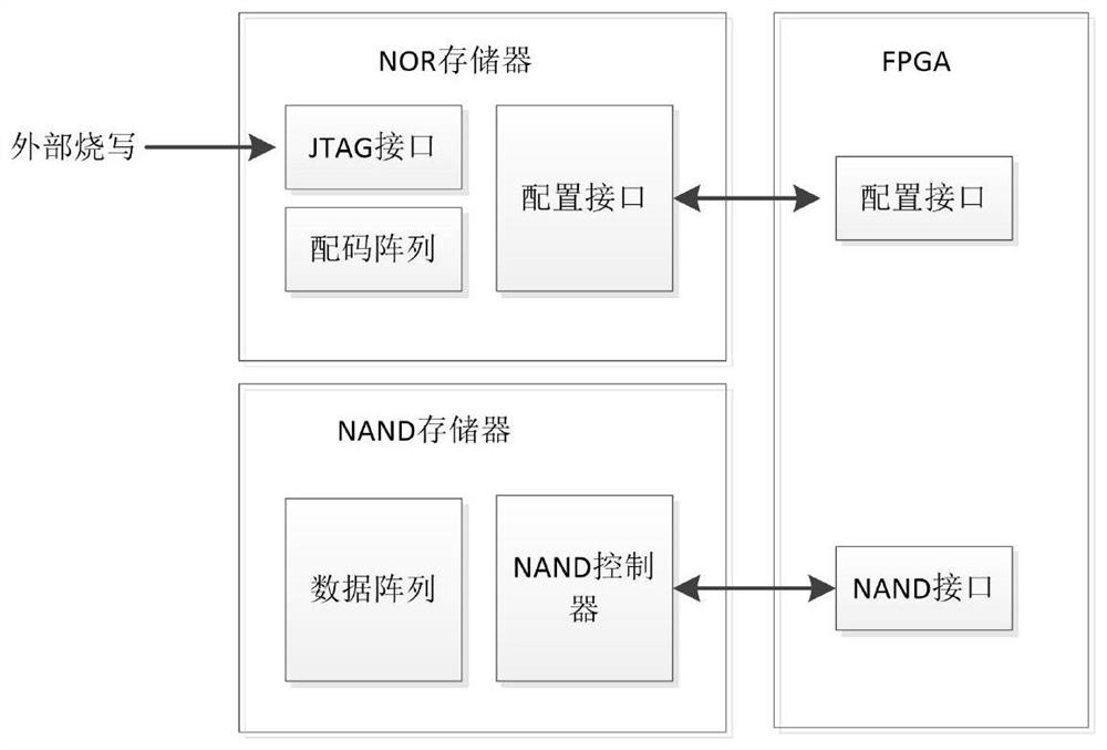
[0050] refer to figure 2 , figure 2 It is a structural schematic diagram of a field programmable logic gate array configuration system in an embodiment of the present invention.

[0051] In this embodiment, the field programmable logic gate array configuration system includes: NAND memory and FPGA.

[0052] The NAND memory includes: a data array, a coding array, a first configuration interface and a NAND controller, the FPGA includes: a second configuration interface and a NAND interface, the second configuration interface is connected to the first configuration interface, The NAND interface is connected with the NAND controller.

[0053] The matching array is used to store multiple versions of matching files.

[0054] The first configuration interface is used to read the first configuration code from the configuration array after power-on, and send the first configuration code to the second configuration interface, so that the FPGA to configure.

[0055] In this embodime...

no. 2 example

[0072] Based on the same inventive idea, such as image 3 As shown, the embodiment of the present invention also provides a configuration method of a field programmable logic gate array, the method is based on a configuration system of a field programmable logic gate array, and the system includes: a NAND memory and an FPGA; wherein the NAND memory includes: A data array, a coding array, a first configuration interface and a NAND controller, the FPGA includes: a second configuration interface and a NAND interface, the second configuration interface is connected to the first configuration interface, and the NAND interface is connected to the The NAND controller connection described above. The methods include:

[0073] Step S10: After the NAND memory is powered on, it reads a first configuration code from the configuration array through the first configuration interface, and sends the first configuration code to the second configuration code of the FPGA. The second is a config...


PUM


Abstract

The invention relates to the technical field of field programmable logic gate arrays, in particular to a configuration system and method of a field programmable logic gate array, and the system comprises an NAND memory and an FPGA; the NAND memory comprises a data array, a code matching array, a first configuration interface and an NAND controller; the FPGA comprises a second configuration interface and an NAND interface, the second configuration interface is connected with the first configuration interface, and the NAND interface is connected with the NAND controller. According to the invention, the code matching file and the access data are stored in the NAND memory together, so that the integration of configuration and storage of the FPGA is achieved, the whole system only needs one external memory, the expenditure of an independent FPGA configuration memory circuit is saved, the board-level area is saved, and the board-level development difficulty is reduced. Meanwhile, due to thelarge-capacity characteristic of the NAND memory, multiple configuration versions can be stored for the FPGA, and the configuration flexibility of the FPGA is improved.

Description

technical field [0001] The invention relates to the technical field of field programmable logic gate arrays, in particular to a configuration system and method for field programmable logic gate arrays. Background technique [0002] Field Programmable Gate Array (Field Programmable GateArray, FPGA) as a flexible and configurable device, with the development of information industry and microelectronics, is more and more used in video image processing, communication field, digital signal processing and other fields, and requires FPGA has multiple functions and stronger data processing capabilities. [0003] Traditional FPGA systems need to be connected with configuration memory and data memory for use together. Its structure is as figure 1 As shown, the configuration memory generally adopts NOR memory, which is used to store the FPGA configuration code. After power-on, the configuration code is transmitted to the FPGA to complete the power-on configuration. The data memory g...

Claims


Application Information

Patent Timeline
IPC IPC(8): G06F15/78G06F13/16
CPCG06F15/7867G06F13/16Y02D10/00
Inventor 呼红阳张君宇张坤霍长兴谢元禄刘璟刘明
Owner INST OF MICROELECTRONICS CHINESE ACAD OF SCI
Features
  • R&D
  • Intellectual Property
  • Life Sciences
  • Materials
  • Tech Scout
  • Unparalleled Data Quality
  • Higher Quality Content
  • 60% Fewer Hallucinations
Learn More