Chip mounting equipment for solid wax

A technology of solid wax and patch, which is applied in the field of optoelectronics, can solve the problems of increased usage of solid wax, poor fluidity of solid wax, and poor flatness of wafers, etc., and achieves good flatness, uniform wax content, and uniform wax distribution.

Pending Publication Date: 2020-09-18
苏州辰轩光电科技有限公司
View PDF0 Cites 5 Cited by
  • Summary
  • Abstract
  • Description
  • Claims
  • Application Information

AI Technical Summary

Problems solved by technology

However, when the existing placement machine adopts solid wax to mount the wafer, because the fluidity of the solid wax is slightly poor, the wax content between the wafer and the workpiece will be uneven, and the flatness of the adhered wafer will be uneven. Good and other questions
In addition, in order to ensure that there is wax on the contact surface between the wafer and the support

Method used


Image

  • Chip mounting equipment for solid wax
  • Chip mounting equipment for solid wax
  • Chip mounting equipment for solid wax

Examples


Embodiment Construction

[0055]The following will clearly and completely describe the technical solutions in the embodiments of the present invention with reference to the accompanying drawings in the embodiments of the present invention. Obviously, the described embodiments are only some, not all, embodiments of the present invention. Based on the embodiments of the present invention, all other embodiments obtained by persons of ordinary skill in the art without making creative efforts belong to the protection scope of the present invention.

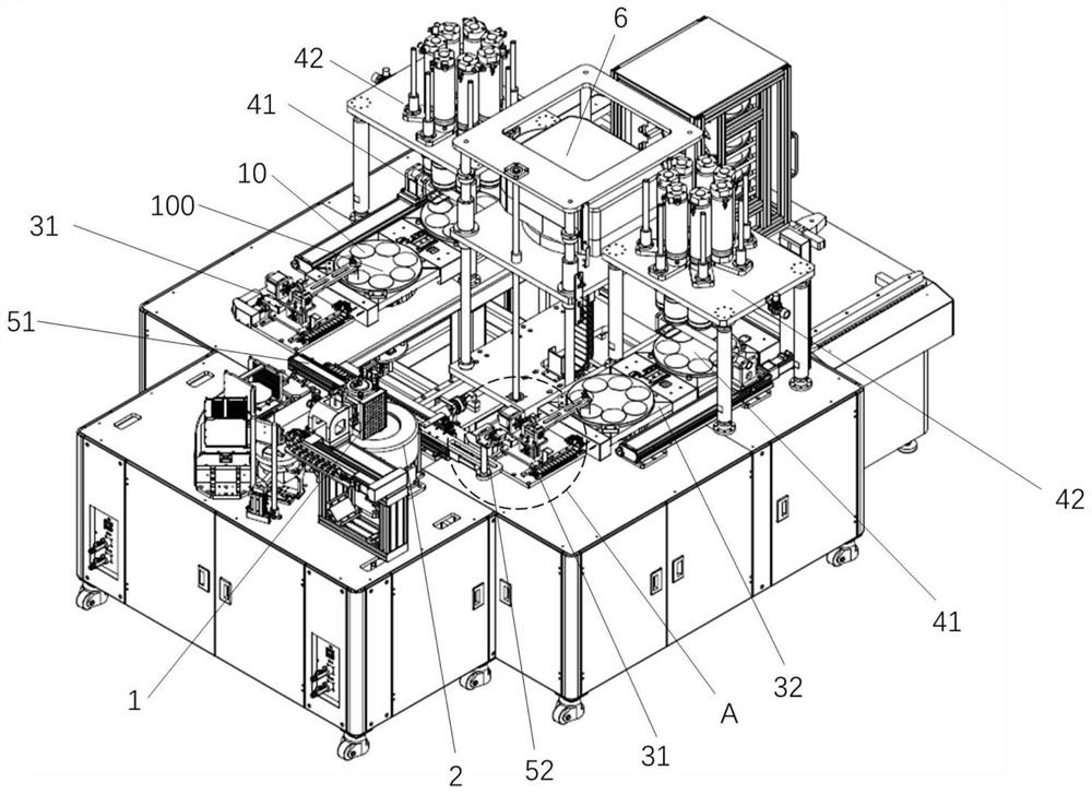
[0056] Such as figure 1 As shown, the placement equipment in this embodiment is used to adhere the wafer 10 on the carrier workpiece 100, the material of the wafer 10 can be sapphire, gallium arsenide and silicon carbide, and the carrier workpiece 100 can be a ceramic disc. Among them, the placement equipment includes:

[0057] The wax dripping device 1 is used for dripping wax to the back of the wafer 10, and the wax in this embodiment refers to solid wax.

...


PUM


Abstract

The invention discloses chip mounting equipment for solid wax. The equipment comprises a wax dripping device, a wax throwing device, a pre-patching device and a pressing and attaching device, whereinthe wax dripping device is used for dripping wax to the back surface of a wafer; the wax throwing device is used for melting wax on the wafer and throwing the wax on the wafer; the pre-patching deviceis used for pre-positioning the wafer subjected to wax throwing on a bearing workpiece; the pressurizing device is used for pressurizing a wafer and a bearing workpiece, therefore, the wafer is adhered to the bearing workpiece, the pressurizing device comprises a third bearing platform and a pressing machine module arranged above the third bearing table, the third bearing platform is used for bearing a bearing workpiece to which a wafer is pre-pasted; the pressing machine module is used for pressurizing the wafer on the bearing workpiece, a third heating mechanism and a cooling mechanism arearranged on the third bearing platform, the third heating mechanism is used for heating wax between the bearing workpiece and the wafer, and the cooling mechanism is used for cooling the wax between the bearing workpiece and the wafer. The scheme has the advantages of saving solid wax, saving consumables such as wax absorbing paper, improving the production efficiency, reducing the mounting spaceand the like.

Description

technical field [0001] The invention relates to the field of optoelectronic technology, in particular to a patch device for solid wax. Background technique [0002] The manufacturing process of the LED chip needs to go through the grinding and thinning process of the wafer. This thinning process can facilitate subsequent chip cutting, packaging and solidification, and improve the heat dissipation performance of the chip during use. Before the wafer thinning process, the wafer needs to be adhered to the specific surface of the workpiece for carrying. The side of the wafer that does not need to be ground is adhered to the carrying workpiece, and the thinning side of the wafer needs to be ground (also called the back of the wafer. ) exposed, in the LED chip manufacturing process, this process of adhering the wafer is called the SMT process. [0003] With the rapid development of the LED chip industry, in order to meet the growing demand for production capacity, automatic place...

Claims


Application Information

Patent Timeline
IPC IPC(8): H01L21/67H01L21/677H01L33/48B05C9/02B05C9/14B05C11/08
CPCB05C9/02B05C9/14B05C11/08H01L21/6715H01L21/67742H01L33/48
Inventor 胡小辉
Owner 苏州辰轩光电科技有限公司
Why Eureka
Try Eureka