A solar silicon chip recovery and reuse processing device

A technology for solar silicon wafers and processing devices, applied to the cleaning method using tools, the cleaning method using gas flow, cleaning methods and appliances, etc., which can solve the problem of single motion state, silicon wafers not being clamped, clamping Part deformation and other problems, to achieve the effect of improving the degree of removal

Active Publication Date: 2022-06-07
马鞍山华鑫财务咨询有限公司
View PDF12 Cites 0 Cited by
  • Summary
  • Abstract
  • Description
  • Claims
  • Application Information

AI Technical Summary

Problems solved by technology

[0003] 1. The method of clamping the silicon wafer with a relatively rigid structure is likely to cause a large deformation of the clamping part of the silicon wafer, and the silicon wafer as a whole cannot receive effective clamping force, and at the same time clean the surface of the silicon wafer The movement state of the structure is relatively simple, and the same one-way movement cleaning method is often used, and this method tends to cause a low degree of cleaning on the surface of the silicon wafer;
[0004] 2. During the cleaning process of the silicon wafer surface, the removed impurities tend to fly around and accumulate on the device structure and re-adsorb on the silicon wafer. However, the adsorbed impurities cannot be collected and processed in a timely and effective manner, and the flying Impurities can also easily have a certain impact on the cooperation and operation of the components

Method used


Image

  • A solar silicon chip recovery and reuse processing device
  • A solar silicon chip recovery and reuse processing device
  • A solar silicon chip recovery and reuse processing device

Examples


Embodiment Construction

[0034] Embodiments of the present invention are described in detail below with reference to the accompanying drawings, but the present invention can be implemented in many different ways as predetermined and covered by the claims.

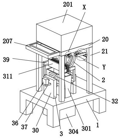
[0035] like Figure 1 to Figure 11 As shown, a solar silicon wafer recycling processing device includes a worktable 1, a clamping mechanism 2 and a cleaning mechanism 3. The upper end surface of the worktable 1 is provided with a clamping mechanism 2, and the left side of the clamping mechanism 2 is installed. A cleaning mechanism 3 is arranged on the side, and the lower end of the cleaning mechanism 3 is connected with the upper end surface of the workbench 1 .

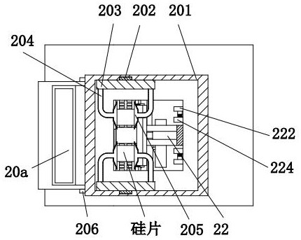
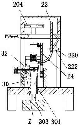
[0036] The clamping mechanism 2 includes a base plate 20 , a bracket 21 , a track plate 22 , a No. 1 electric slider, a support rod 24 and a clamping assembly 25 . The brackets 21 are installed symmetrically, and the brackets 21 are arranged symmetrically on the left and right sides. A r...


PUM


Abstract

The invention relates to a solar silicon chip recovery and reuse processing device, which includes a workbench, a clamping mechanism and a cleaning mechanism. The upper end of the workbench is equipped with a clamping mechanism, and the left side of the clamping mechanism is provided with a cleaning mechanism. The lower end of the cleaning mechanism is connected to the upper surface of the workbench. This invention adopts the design concept of multiple cleaning structures to recycle and reuse solar silicon wafers. The cleaning degree of the surface of the silicon wafer is also provided with a centralized treatment and collection structure for removing impurities.

Description

technical field [0001] The invention relates to the technical field of silicon wafer processing, in particular to a device for recycling and reusing solar silicon wafers. Background technique [0002] The content of silicon in the earth's crust reaches 25.8%, which provides an inexhaustible source for the production of single crystal silicon. Since silicon is one of the most abundant elements in the earth's crust, it is destined to enter the large-scale market for solar cells. In terms of products, the advantage of reserves is also one of the reasons why silicon has become the main material of photovoltaics. Crystalline silicon solar cells have excellent characteristics such as high efficiency, low attenuation, and strong reliability. Silicon wafers are important materials for making integrated circuits. Photolithography, ion implantation and other methods can be used to make various semiconductor devices. The demand for semiconductor-grade polysilicon is 19,000 tons, which ...

Claims


Application Information

Patent Timeline
Patent Type & Authority Patents(China)
IPC IPC(8): B08B1/00B08B5/02B08B13/00B08B15/04
CPCB08B1/002B08B5/02B08B13/00B08B15/04Y02P70/50
Inventor 卜敬翔
Owner 马鞍山华鑫财务咨询有限公司
Why Eureka
Try Eureka