Preparation method of semiconductor/superconductor heterojunction nanowire network

A semiconductor and superconductor technology, applied in nanostructure manufacturing, nanotechnology, nanotechnology, etc., can solve the difficulties in obtaining high-quality semiconductor/superconductor heterojunction interfaces, stacking faults and twin defects, lattice mismatch, etc. problems, to achieve the effects of good size controllability, high crystal quality, and easy device processing

Active Publication Date: 2020-09-25
INST OF SEMICONDUCTORS - CHINESE ACAD OF SCI
View PDF7 Cites 2 Cited by
  • Summary
  • Abstract
  • Description
  • Claims
  • Application Information

AI Technical Summary

Problems solved by technology

In the process of preparing planar InAs and InSb nanowire networks by selective epitaxy, due to the large lattice mismatch between the InAs and InSb nanowires and the III-V semiconductor substrate, this will cause the occurrence of InAs and InSb nanowire networks. A large number of stacking faults and twin defects make it difficult to obtain high-quality semiconductor / superconductor heterojunction interfaces

Method used


Image

  • Preparation method of semiconductor/superconductor heterojunction nanowire network
  • Preparation method of semiconductor/superconductor heterojunction nanowire network

Examples


Embodiment Construction

[0028] In order to make the object, technical solution and advantages of the present invention clearer, the present invention will be further described in detail below in conjunction with specific embodiments and with reference to the accompanying drawings.

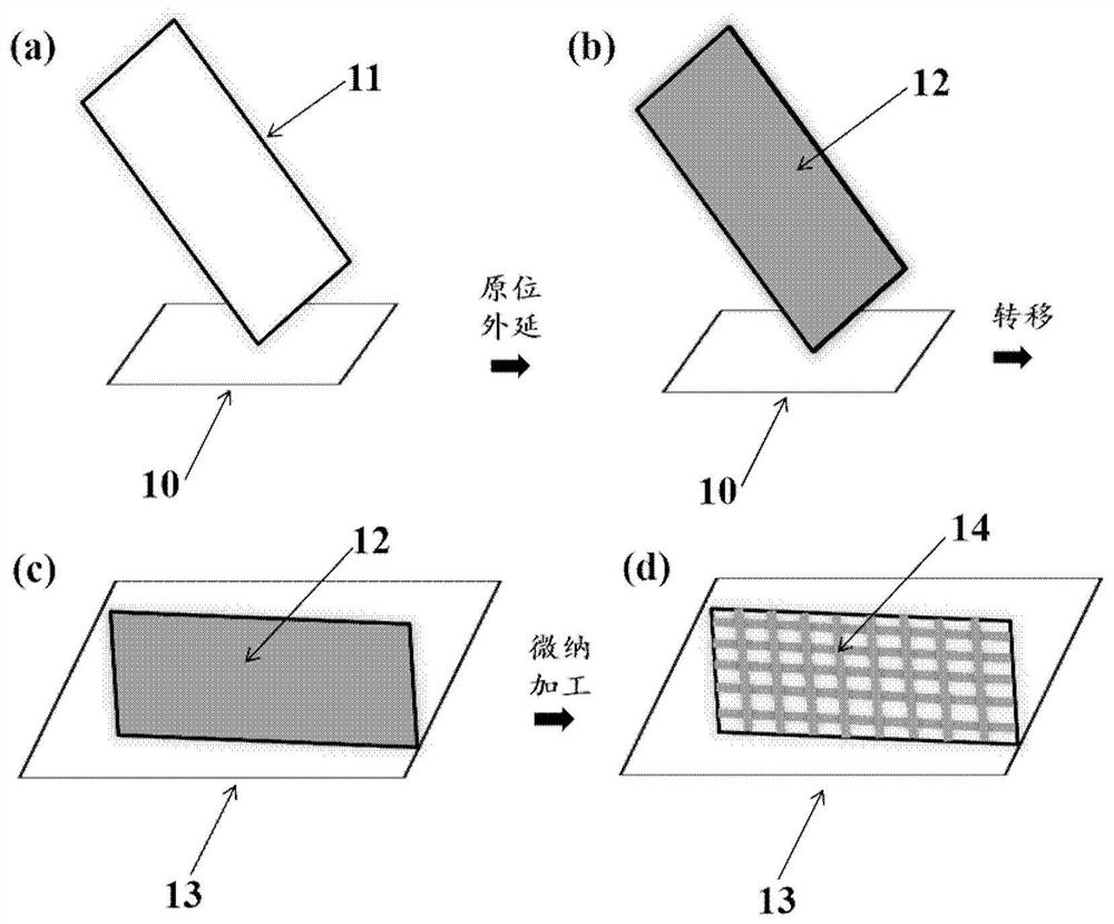
[0029] figure 1 A schematic flowchart of a method for preparing a semiconductor / superconductor heterojunction nanowire network according to an embodiment of the present invention is schematically shown. The semiconductor / superconductor heterojunction refers to the combination of two different materials, semiconductor and superconductor, forming a heterojunction at the interface.

[0030] Such as figure 1 As shown, the preparation method of the semiconductor / superconductor heterojunction nanowire network may include the following operations (a) to (d).

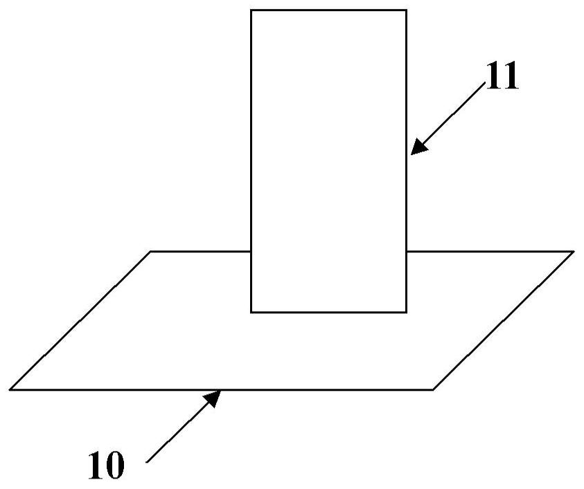
[0031] (a) Vertical semiconductor nanosheets 11 are prepared on the first substrate 10 .

[0032] According to an embodiment of the present invention, the material of t...


PUM


Abstract

The invention provides a preparation method of a semiconductor / superconductor heterojunction nanowire network. The preparation method comprises the following steps: preparing a vertical semiconductornanosheet on a first substrate; performing in-situ epitaxy of a superconductor on the semiconductor nanosheet to obtain a semiconductor nanosheet with the superconductor epitaxy; transferring the semiconductor nanosheet on which the superconductor is extended to a second substrate; processing an in-situ epitaxial superconductor on a semiconductor nanosheet into a nanowire network by utilizing micro-nano processing to obtain a semiconductor / superconductor heterojunction nanowire network.

Description

technical field [0001] The invention relates to a semiconductor material preparation technology, mainly a method for preparing a semiconductor / superconductor heterojunction nanowire network. Background technique [0002] Fault-tolerant topological quantum computing based on Majorana fermions is a solution proposed and recognized in recent years to solve the problem of quantum computer error correction. The detection and finding of Majorana fermions is the key to its use in fault-tolerant topological quantum computing. The Sarma research group of the University of Maryland [Phys.Rev.Lett., 104(2010) 040502] and the Oreg research group of the Weizmann Institute of Science [Phys.Rev.Lett., 105(2010) 077001] theoretically predicted: In a strong magnetic field, a superconductor and a narrow bandgap semiconductor (InAs or InSb) nanowire are used to form a P-wave superconducting chain. Due to the proximity effect of the superconductor, the nanowire can form an effective P-wave pair...

Claims


Application Information

Patent Timeline
IPC IPC(8): B82B3/00B82Y10/00
CPCB82B3/0014B82Y10/00
Inventor 潘东赵建华
Owner INST OF SEMICONDUCTORS - CHINESE ACAD OF SCI
Why Eureka
Try Eureka