A preparation method of field emission transistor, field emission transistor and equipment

A field emission and transistor technology, applied in the manufacture of discharge tubes/lamps, components of discharge tubes/lamps, control electrodes, etc., can solve the problems that field emission transistors cannot be arrayed, and achieve good local electric field enhancement, Effects of Improving Emission Current and Current Stability

Active Publication Date: 2021-07-27
SHANGHAI INST OF MICROSYSTEM & INFORMATION TECH CHINESE ACAD OF SCI
View PDF0 Cites 0 Cited by
  • Summary
  • Abstract
  • Description
  • Claims
  • Application Information

AI Technical Summary

Problems solved by technology

[0005] The technical problem to be solved by the present invention is that the existing field emission transistor preparation method cannot realize the problem of array type emission tips

Method used


Image

  • A preparation method of field emission transistor, field emission transistor and equipment
  • A preparation method of field emission transistor, field emission transistor and equipment
  • A preparation method of field emission transistor, field emission transistor and equipment

Examples


Embodiment Construction

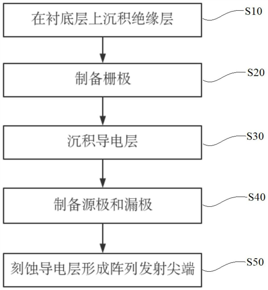
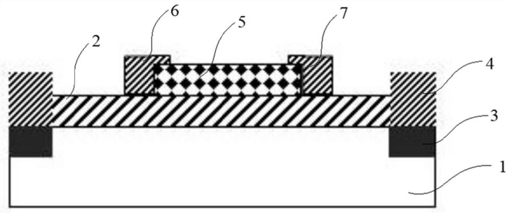
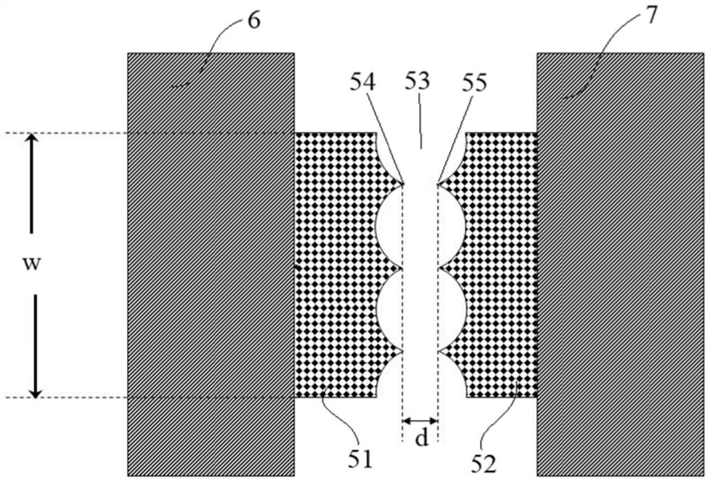
[0031] The technical solutions in the embodiments of the present application will be clearly and completely described below in conjunction with the drawings in the embodiments of the present application. Apparently, the described embodiments are only some of the embodiments of this application, not all of them. Based on the embodiments in this application, all other embodiments obtained by persons of ordinary skill in the art without creative efforts fall within the protection scope of this application.

[0032] Reference herein to "one embodiment" or "an embodiment" refers to a specific feature, structure or characteristic that may be included in at least one implementation of the present application. In the description of the present application, it should be understood that the orientation or positional relationship indicated by the terms "upper", "lower", "top", "bottom" etc. is based on the orientation or positional relationship shown in the drawings, and is only for It ...


PUM

PropertyMeasurementUnit
thicknessaaaaaaaaaa
thicknessaaaaaaaaaa

Abstract

The present invention relates to the field of semiconductor devices, in particular to a method for preparing a field emission transistor, a field emission transistor and equipment, comprising: preparing a base layer; wherein, a gate is provided on the base layer; and a conductive electrode is deposited on the base layer. layer; depositing a source electrode and a drain electrode at both ends of the conductive layer; etching the conductive layer to obtain an emission tip; wherein, the etching method is focused ion beam etching. The preparation method of the field emission transistor described in this application can realize an array type emission tip, which is beneficial to improve the overall emission current and current stability. And after focused ion beam etching, a smaller emission tip can be formed, and the local electric field enhancement effect is better.

Description

technical field [0001] The invention relates to the field of semiconductor devices, in particular to a method for preparing a field emission transistor, a field emission transistor and equipment. Background technique [0002] Field emission transistor is a new type of transistor produced by the fusion of vacuum tube technology, semiconductor technology and nanotechnology. Because of its fast response, high temperature resistance and radiation resistance, it has great application potential in extreme environments such as aerospace and deep sea exploration. , and is expected to be applied in the field of Terahertz (Tera Hertz, THz) technology. [0003] In a field emission transistor, a sufficiently strong electric field (usually around 10 7 V / cm or more), this electric field reduces and narrows the potential barrier between cathode electrons and the vacuum level, the probability of electrons entering the vacuum through the tunneling mechanism is significantly increased, and a...

Claims


Application Information

Patent Timeline
Patent Type & Authority Patents(China)
IPC IPC(8): H01J9/02H01J1/304H01J1/46
CPCH01J1/3042H01J1/46H01J9/02H01J9/025
Inventor 刘梦王跃林李铁
Owner SHANGHAI INST OF MICROSYSTEM & INFORMATION TECH CHINESE ACAD OF SCI
Why Eureka
Try Eureka