
Acoustic emission monitoring and endpoint for chemical mechanical polishing

A chemical machinery and grinding pad technology, applied in grinding machine tools, grinding tools, grinding devices, etc., can solve the problem of unable to meet the increasing demand of semiconductor device manufacturers, and achieve the effect of improving consistency

Active Publication Date: 2020-10-02
APPLIED MATERIALS INC
View PDF9 Cites 0 Cited by
  • Summary
  • Abstract
  • Description
  • Claims
  • Application Information

AI Technical Summary

Problems solved by technology

However, existing monitoring technologies may not be able to meet the increasing demands of semiconductor device manufacturers

Method used


Image

  • Acoustic emission monitoring and endpoint for chemical mechanical polishing
  • Acoustic emission monitoring and endpoint for chemical mechanical polishing
  • Acoustic emission monitoring and endpoint for chemical mechanical polishing

Examples


Embodiment Construction

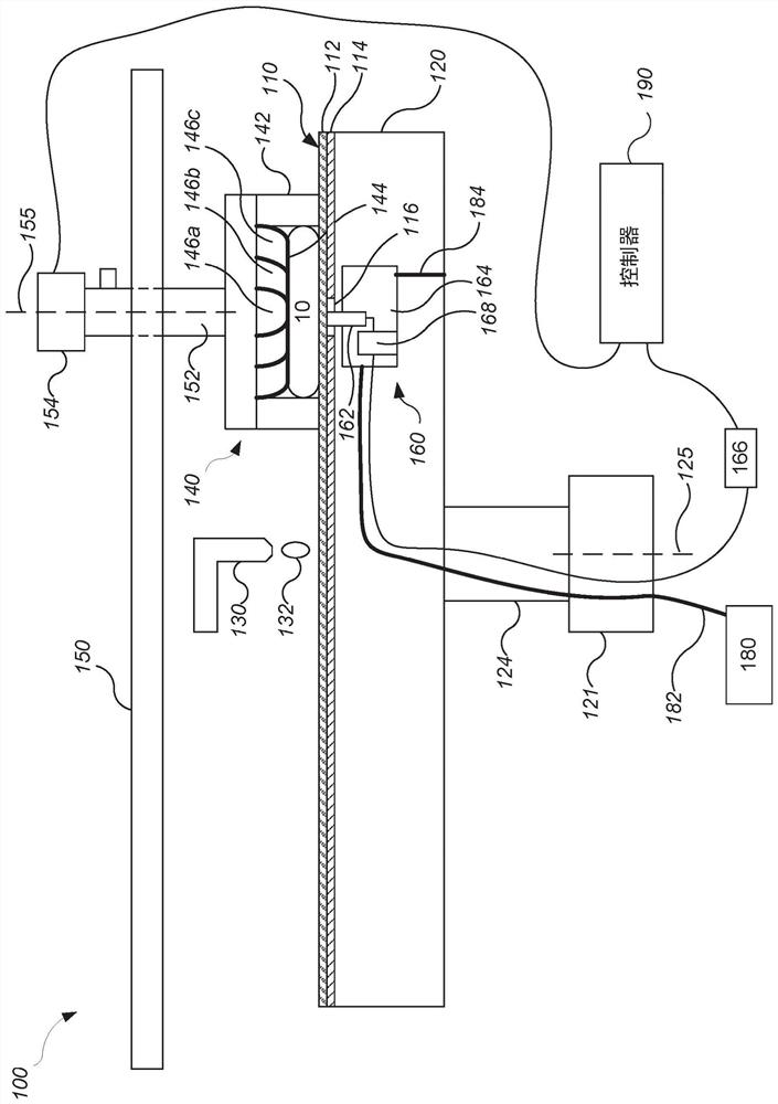
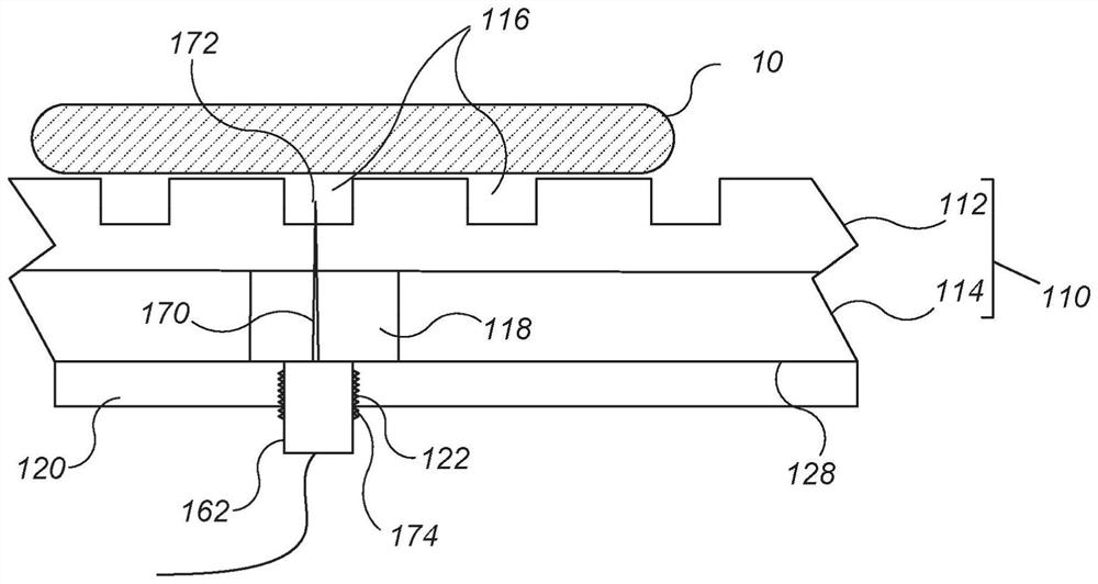
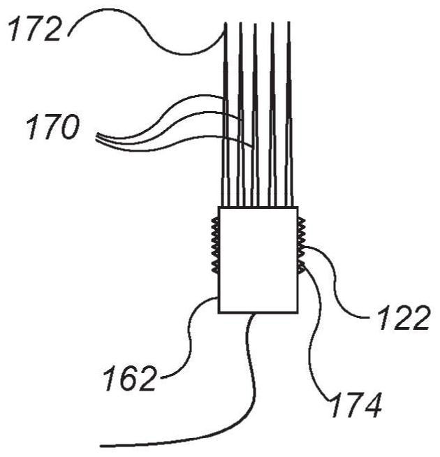
[0031] In some semiconductor chip fabrication processes, overlying layers (eg, metal, silicon oxide, or polysilicon) are ground until underlying layers (eg, dielectrics such as silicon oxide, silicon nitride, or high-K dielectrics) are exposed. For some applications, the acoustic emission from the substrate will change when the undercoat is exposed. The end of grinding can be determined by detecting this change in the acoustic signal.

[0032] The acoustic emission to be monitored may be caused by stress energy when the substrate material is deformed, and the resulting acoustic spectrum is related to the material properties of the substrate. It may be noted that this acoustic effect is not the same as the noise (sometimes referred to as the acoustic signal) produced by the substrate rubbing against the polishing pad; the acoustic effect occurs in a significantly higher frequency range than such rubbing noise, e.g., 50kHz to 1 MHz, and thus the monitoring of a suitable frequen...


PUM


Abstract

A chemical mechanical polishing apparatus includes a platen to support a polishing pad, and an in-situ acoustic emission monitoring system including an acoustic emission sensor supported by the platen, a waveguide configured to extending through at least a portion of the polishing pad, and a processor to receive a signal from the acoustic emission sensor. The in-situ acoustic emission monitoring system is configured to detect acoustic events caused by deformation of the substrate and transmitted through the waveguide, and the processor is configured to determine a polishing endpoint based on the signal.

Description

[0001] This application is a divisional application of an invention patent application with an application date of February 5, 2016, an application number of "201680013942.0", and an invention title of "Acoustic Emission Monitoring and Endpoint for Chemical Mechanical Polishing". technical field [0002] The present disclosure relates to in-situ monitoring of chemical mechanical polishing. Background technique [0003] Integrated circuits are usually formed on a substrate by sequentially depositing conductive, semiconducting or insulating layers on a silicon wafer. One fabrication step involves depositing a filler layer on a non-planar surface and planarizing the filler layer. For certain applications, the filler layer is planarized until the top surface of the patterned layer is exposed. For example, a conductive filler layer can be deposited on a patterned insulating layer to fill trenches or holes in the insulating layer. After planarization, the portions of the metal l...

Claims


Application Information

Patent Timeline
Patent Type & Authority Applications(China)
IPC IPC(8): B24B37/013B24B37/04B24B37/10B24B37/20B24B49/00
CPCB24B37/013B24B49/003B24B37/042B24B37/10B24B37/20
Inventor J·唐D·M·石川B·切里安J·吴T·H·奥斯特赫尔德
Owner APPLIED MATERIALS INC
Features
  • Generate Ideas
  • Intellectual Property
  • Life Sciences
  • Materials
  • Tech Scout
  • Unparalleled Data Quality
  • Higher Quality Content
  • 60% Fewer Hallucinations
Learn More