Low-voltage IC test for defect screening

a low-voltage ic and defect screening technology, applied in the direction of electrochemical generators, instruments, batteries, etc., can solve the problems of increasing the level of electromigration and other reliability problems, damage to shorted circuits as well as microelectronic circuits in its vicinity, and reducing the defect signal. , the effect of strong maverick signal

Inactive Publication Date: 2014-07-03
ALSEPHINA INNOVATIONS INC
View PDF6 Cites 32 Cited by
  • Summary
  • Abstract
  • Description
  • Claims
  • Application Information

AI Technical Summary

Benefits of technology

[0011]The system and method makes use of low voltage (or “Low V”) current measurements, to measure network currents and a standard parametric measure of a chip's speed or inherent current leakage level. The low voltage currents are then compared to the inherent normalized currents by ring delay and set limits to screen out mavericks. A class of short defects resulting in reliability fails shows a stronger maverick signal when tested at Low V than nominal V and are thus more detectable. Testing at Low V has the benefit of not ablating the problem defect and reducing the defect signal, and also keeps the FET and junction leakage currents low thus keeping the inherent chip leakage level low.

Problems solved by technology

In the field the defect can continue to draw current and create localized heating.
The current drawn can create increased levels of electromigration and other reliability problems.
Localized heating can then, over time, damage the shorted circuit as well as microelectronic circuits in its vicinity.
Smaller wires are more susceptible to opens or shorts due to stress and electromigration which are accelerated by heat and higher current density.
Smaller device / circuit spaces are more susceptible to shorting from metal being extruded due to the above stresses.
Conventional current leakage screens performed in microelectronic testing typically have problems that are two fold: 1) at operating voltages there is low sensitivity to “medium” level shorts defects; 2) shorts defects can have such high current densities that parts of the redundant power and ground wiring can become ablated at operating or higher voltages thus decreasing the current pulled from the power supplies but still pull enough power to cause local heating.
Currently, it is difficult to screen these “medium current” defects that do not cause functional or power limit fails while taking a minimum in yield loss.
This can be especially problematic in arrays or other circuits where redundancy is employed to allow chips with defective arrays or circuits to be usable in the field.
These defects can also be shorting circuits together and pulling substantial currents even if they are not needed for the chip to function.

Method used


Image

  • Low-voltage IC test for defect screening
  • Low-voltage IC test for defect screening
  • Low-voltage IC test for defect screening

Examples


Embodiment Construction

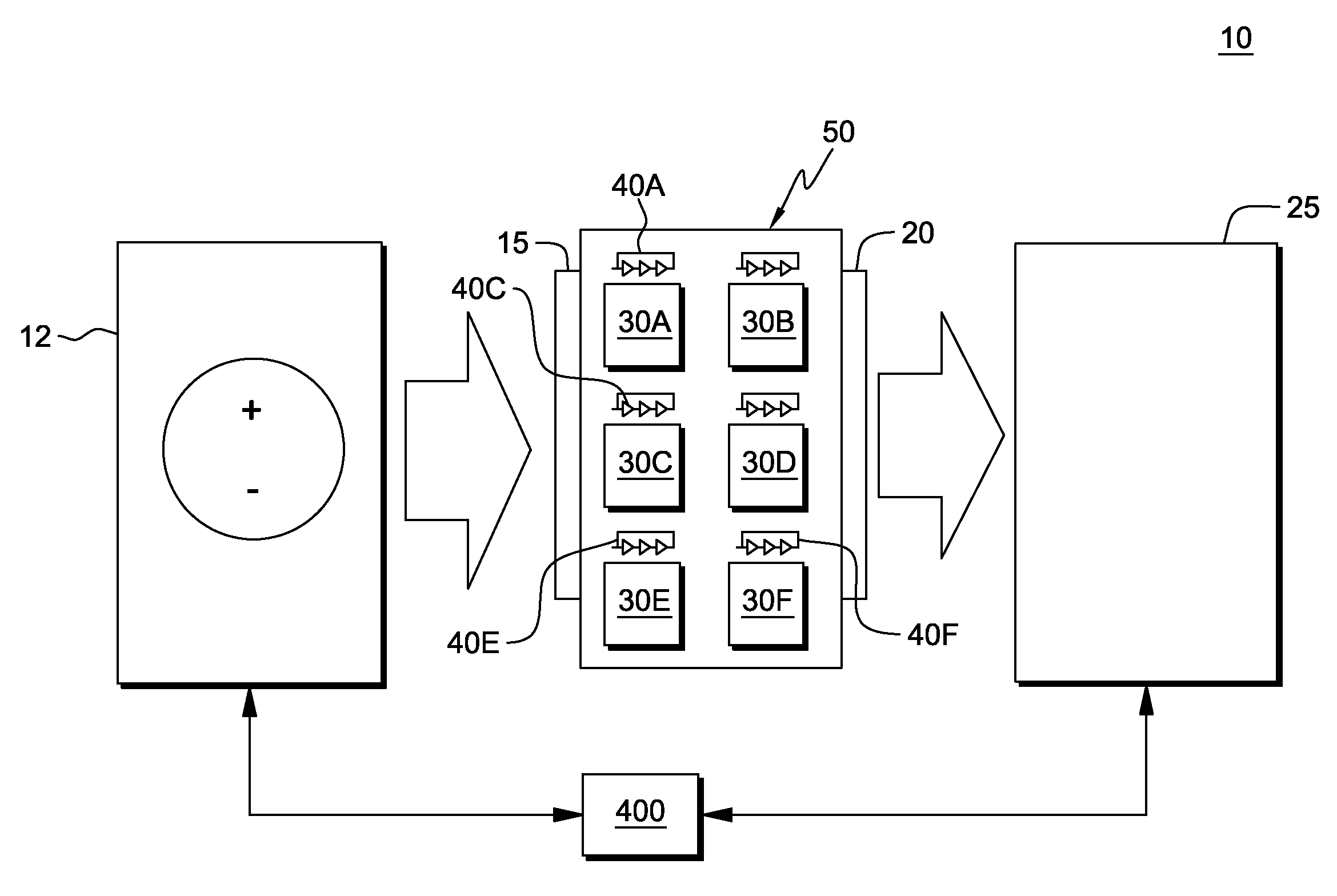
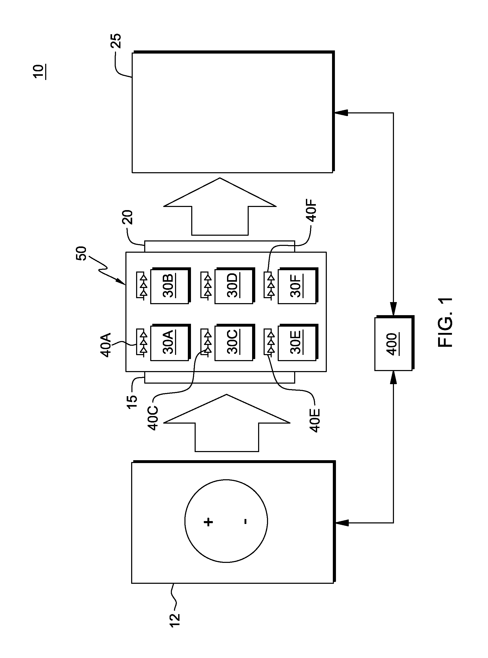
[0035]In one embodiment, the system and method for low voltage defect screening includes utilizing a low voltage current measurement at the beginning of a testing sequence. In one aspect, this is done to protect tester-to-product probing hardware from harmfully high currents. In one embodiment, this applied low voltage is below the threshold voltage of the FETs in the circuits. Resolution is also helped by testing at a lower temperature where less leakage currents are drawn. The low voltage does not therefore turn on FET gated leakage paths thus making shorts defects between power and ground more detectable from the background leakage. The low voltage also decreases the current densities through the power and ground wiring to the shorts defects often preventing these wires from ablation.

[0036]In a further aspect, a current screen may then be subsequently used to sort as failures chips that have greater than a defined current limit. Current limits are normalized by a parameter that c...


PUM


Abstract

System and method using low voltage current measurements to measure voltage network currents in an integrated circuit (IC). In one aspect, a low voltage current leakage test is applied voltage networks for the IC or microchip via one or more IC chip connectors. One or multiple specifications are developed based on chip's circuit delay wherein a chip is aborted or sorted into a lesser reliability sort depending whether the chip fails specification. Alternately, a low voltage current leakage test begins an integrated circuit test flow. Then there is run a high voltage stress, and a second low voltage current leakage test is thereafter added. Then, there is compared the second low voltage test to the first low V test, and if the measured current is less on second test, this is indicative of a defect present which may result in either a scrap or downgrade reliability of chip.

Description

BACKGROUND[0001]This present disclosure relates to systems and methods for preventing defects in microelectronic integrated circuits (IC) and particularly, a low voltage IC test system and method for defect screening of ICs for the purposes of preventing defects in microelectronic circuits from getting into the field where they can cause reliability fails.[0002]Depending on where a defect lands in the fabrication of semiconductors it is possible that the defect can cause shorting from power to ground and not affect signal lines (e.g., “shorts defects”). Thus an impacted chip can be fully functional and pass all structural and functional testing. These chips can then be sorted as a good and sold into the field. In the field the defect can continue to draw current and create localized heating. The current drawn can create increased levels of electromigration and other reliability problems. Localized heating can then, over time, damage the shorted circuit as well as microelectronic cir...

Claims


Application Information

Patent Timeline
Patent Type & Authority Applications(United States)
IPC IPC(8): G01R31/28
CPCG01R31/2851G01R31/2853G01R31/30Y02E60/10H01L21/00H01L24/00H01M2200/00
Inventor POINDEXTER, DANIEL J.CRAFTS, JAMES M.GREENE, KARRE M.LAVALLEE, KENNETH A.STEVENS, KEITH C.
Owner ALSEPHINA INNOVATIONS INC
Why Eureka
Try Eureka