Method and system for accurately measuring bending strain of flexible electronic device

A flexible electronic device and measurement method technology, applied in the direction of electric/magnetic solid deformation measurement, electromagnetic measurement device, etc., can solve the problems of interface slip failure, poor thermal resistance, damage to flexible electronic devices, etc., to achieve true strain consistency, correction Inherent bias, the effect of reducing neutral layer shift

Active Publication Date: 2020-10-16
HUAZHONG UNIV OF SCI & TECH
View PDF20 Cites 4 Cited by
  • Summary
  • Abstract
  • Description
  • Claims
  • Application Information

AI Technical Summary

Problems solved by technology

However, there are certain limitations in the preparation of corresponding strained layers on flexible electronic substrates. For example, metal strained layers generally need to be carried out in a high-temperature environment, so it cannot be used in ordinary films with PDMS (polydimethylsiloxane) with poor heat resistance. alkane) as the substrate of flexible electronics, the preparation process is also vulnerable to the size limit of flexible electronic devices or even damage the flexible electronic devices, which does not have wide applicability and portability, so the use of ultra-thin strain sensors with packaged flexible substrates has become the main test A means of bending performance in flexible electronics
[0004] However, when testing with ultra-thin strain sensors, there are still some problems in the strain measurement of flexible electronic devices: how to ensure that due to the sensitivity of the adhesive layer, the contact between the ultra-thin strain sensor and the flexible electronic device is The interface is very likely to have a slip failure mode, which leads to test results that cannot truly reflect the real bending strain of the flexible electronic device; This leads to the offset problem of the neutral layer of the flexible electronic device to be tested, which causes the strain of the sensing grid to be different from the strain on the outer surface of the device to be tested; To ensure the integrity of no residual bubbles, ultra-thin viscous layer and ultra-thin devices can be obtained, so as to ensure the accuracy of the test, so accurate measurement of the true bending strain of flexible electronic devices is an urgent problem to be solved
For these problems, there are already some solutions, such as Yewang Su et al. (Chen, Y.*; Su, Y.*, Adhesion-Free Thin-Film-LikeCurvature Sensors Integrated on Flexible and Wearable Electronics for Monitoring Bending of Joints and Various Body Gestures.Advanced Materials Technologies, 2019,4(2):1800327.) Considering the influence of interface sliding between ultra-thin strain sensors and flexible electronic devices during the test, a double-layer strain sensor is designed to test flexible electronics. However, the This method is only suitable for cases where the interface slides slightly
At the same time, patents (patents 109505838A, CN 204944424, CN 104944424) consider the influence of the adhesive layer, and propose a push-and-extrusion chip placement device to solve the problem of the uniformity, thickness, and absence of the adhesive layer during the test process when the strain sensor is mounted. problems such as air bubbles and impurities, but this method is only suitable for flexible strain sensors with large plane type, stiffness, and thickness, and is not suitable for the measurement of ultra-thin flexible sensors and flexible electronic devices under curved surface morphology; another example is the patent CN102001617A proposed A displacement loading method for flexible electronic devices to correct the influence caused by loading factors. However, this method only considers the influence of loading factors, and does not consider the influence of factors such as the adhesive layer and the thickness of flexible electronic devices, especially for ultra-thin flexible electronics. It is necessary to ensure that the adhesive layer is thinner, so that the neutral layer shift is small

Method used


Image

  • Method and system for accurately measuring bending strain of flexible electronic device
  • Method and system for accurately measuring bending strain of flexible electronic device
  • Method and system for accurately measuring bending strain of flexible electronic device

Examples


Embodiment Construction

[0036] In order to make the object, technical solution and advantages of the present invention clearer, the present invention will be further described in detail below in conjunction with the accompanying drawings and embodiments. It should be understood that the specific embodiments described here are only used to explain the present invention, not to limit the present invention. In addition, the technical features involved in the various embodiments of the present invention described below can be combined with each other as long as they do not constitute a conflict with each other.

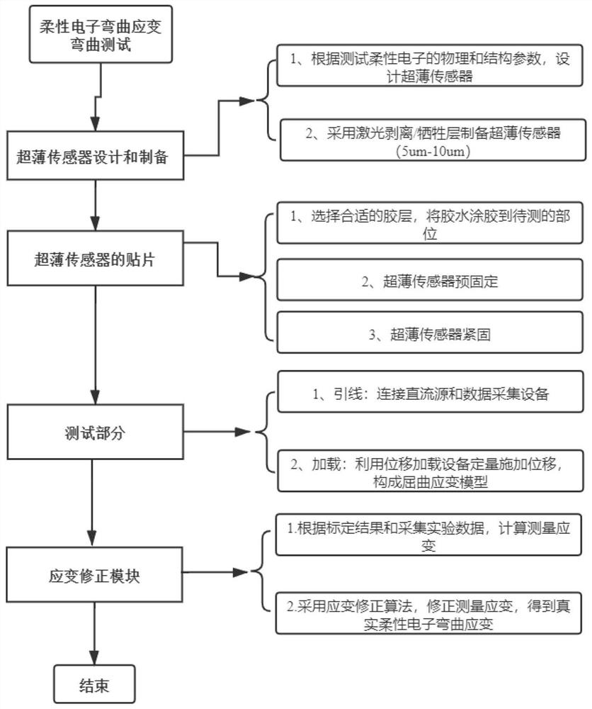
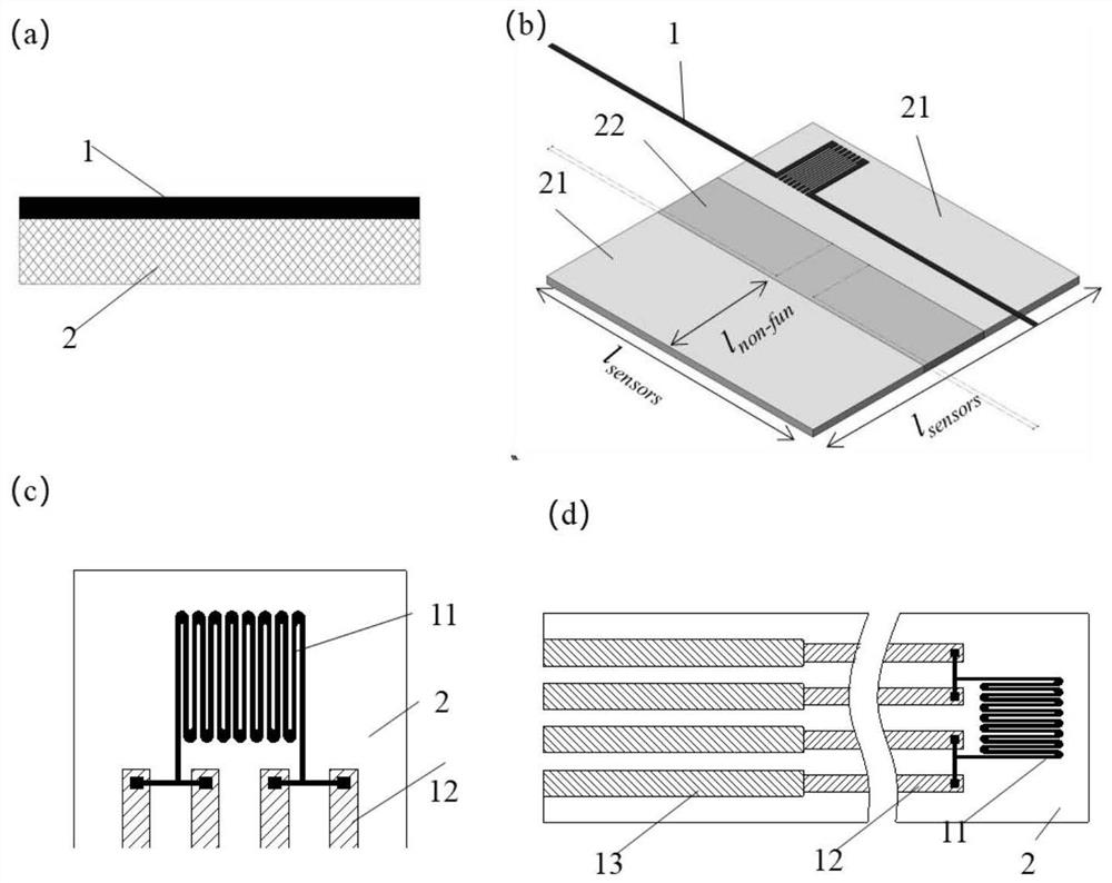
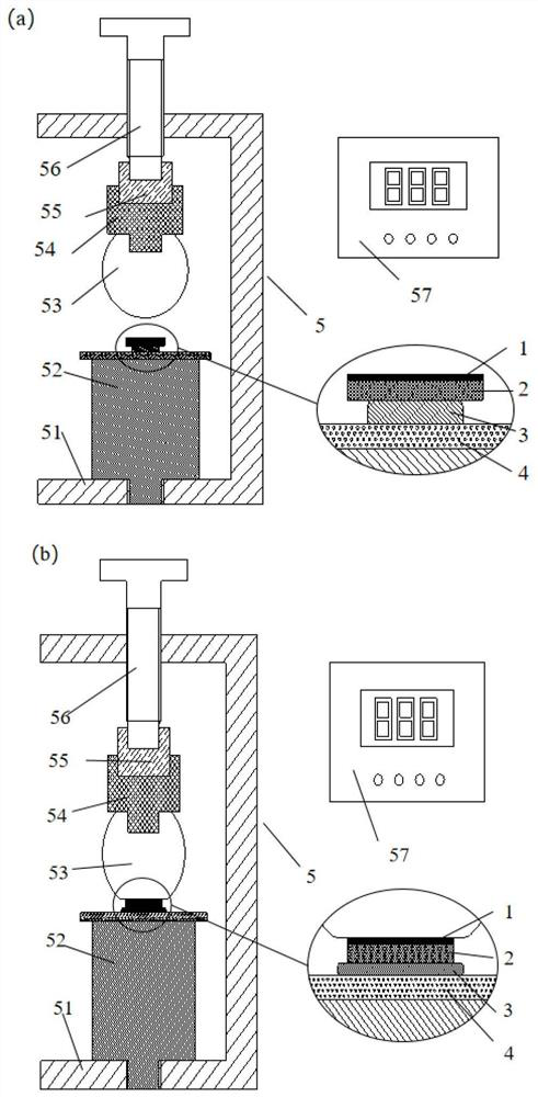
[0037] see figure 1 and figure 2 The method for accurately measuring the bending strain of flexible electronic devices provided by the present invention includes the design and preparation of ultra-thin strain sensors, the placement of ultra-thin strain sensors (gluing on the side, pre-mounting, fastening), flexible electronic device test modules ( Leads, loading), and strain correction modul...


PUM


Abstract

The invention belongs to the related technical field of flexible electronic testing, and discloses a method and a system for accurately measuring bending strain of a flexible electronic device, and the method comprises the following steps: (1), providing an ultrathin strain sensor; (2) pre-fixing the ultra-thin strain sensor on the flexible electronic device through glue, clamping the ultra-thin strain sensor and the flexible electronic device to extrude redundant glue, and then finishing fastening of the ultra-thin strain sensor after the glue is cured; (3) integrally connecting the ultrathinsensor and the flexible electronic device to a test device, and performing loading measurement to acquire multiple groups of experimental data; and (4) calculating the dependent variable of the ultrathin strain sensor in the buckling process according to the strain coefficient of the ultrathin strain sensor and the obtained experimental data, and then correcting the obtained dependent variable byadopting the modified positive coefficient, so as to obtain the real strain of the flexible electronic device to be measured. According to the invention, the measurement accuracy is improved, and theapplicability is good.

Description

technical field [0001] The invention belongs to the technical field related to flexible electronic testing, and more specifically, relates to a precise measurement method and system for bending strain of flexible electronic devices. Background technique [0002] Flexible electronic devices, such as flexible display screens, structural health monitoring equipment, aircraft smart skins, electronic skins, and flexible solar cells, have subversively changed the rigidity of traditional information devices because they can withstand large deformations such as bending, torsion, and folding. The physical form realizes the wearability and implantability of traditional electronic products, conformal contact and perfect integration with the human body, and is the strategic commanding height of future information. With the increasing importance of flexible electronic devices, people have higher and higher requirements for their mechanical properties. Especially in the working environme...

Claims


Application Information

Patent Timeline
Patent Type & Authority Applications(China)
IPC IPC(8): G01B7/16
CPCG01B7/18
Inventor 黄永安侯超陈福荣
Owner HUAZHONG UNIV OF SCI & TECH
Why Eureka
Try Eureka