SRAM storage space allocation method and device for and chip

A storage space and allocation method technology, applied in the computer field, can solve the problems of low utilization rate of SRAM storage space, inflexible storage space allocation, increase of SRAM area, etc., to achieve the effect of improving flexibility, reducing wiring difficulty, and reducing area

Active Publication Date: 2020-10-16
新华三半导体技术有限公司
View PDF12 Cites 1 Cited by
  • Summary
  • Abstract
  • Description
  • Claims
  • Application Information

AI Technical Summary

Problems solved by technology

The storage space allocation of this SRAM is not flexible enough, and it is easy to cause the actual allocated SRAM storage space to be much larger than the SRAM storage space actually required by the communication equipment, and the SRAM storage space utilizatio

Method used


Image

  • SRAM storage space allocation method and device for and chip
  • SRAM storage space allocation method and device for and chip
  • SRAM storage space allocation method and device for and chip

Examples


Embodiment Construction

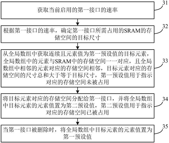
[0064] The following will clearly and completely describe the technical solutions in the embodiments of the application with reference to the drawings in the embodiments of the application. Apparently, the described embodiments are only some of the embodiments of the application, not all of them. Based on the embodiments in this application, all other embodiments obtained by persons of ordinary skill in the art without making creative efforts belong to the scope of protection of this application.

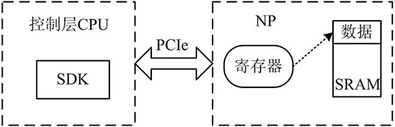
[0065] SRAM is part of the chip. The chip can be NP (Network Processor, network processing chip), and the chip can also be other chips, such as DSP (Digital Signal Processor, digital signal processing chip), ASIC (Application Specific Integrated Circuit, application specific integrated circuit), FPGA (Field-Programmable Gate Array, Field Programmable Gate Array) or other programmable logic devices, discrete gate or transistor logic devices, discrete hardware components. This embodi...


PUM


Abstract

The embodiment of the application provides an SRAM storage space allocation method and device and a chip. The method comprises the steps: determining the target size of storage space, needing to be occupied by a first interface, of an SRAM according to the rate of a currently started first interface; acquiring continuous target elements with element values being first preset values from a global array, the size sum of the storage spaces corresponding to the target elements being larger than or equal to the target size, and the first preset values being used for indicating that the corresponding storage spaces are not occupied; allocating a storage space corresponding to the target element to the first interface, and setting an element value of the target element in the global array as a second preset value, the second preset value indicating that the storage space is occupied; and when the first interface is deleted, setting the element value of the target element in the global array as a first preset value. By applying the technical scheme provided by the embodiment of the invention, the storage space allocation flexibility of the SRAM is improved, the storage space utilization rate of the SRAM is improved, the area of the SRAM is reduced, and the wiring difficulty of back-end development is reduced.

Description

technical field [0001] The present application relates to the field of computer technology, in particular to a method, device and chip for allocating storage space of an SRAM. Background technique [0002] With the broadband of the Internet and the high-speed of the local area network, a large amount of data communication is required between communication devices, so the demand for high-speed, large-capacity data buffering becomes more and more urgent. SRAM (Static Random-Access Memory) is a kind of memory with static access function, which is characterized by the function of saving data without refreshing the circuit. SRAM uses transistors to store data, and it does not need a refresh circuit, which makes the working performance of the entire memory higher than that of dynamic random access memory. Therefore, SRAM can well meet the demand for high-speed, large-capacity data buffering, and then SRAM is widely used in communication equipment. [0003] Although SRAM has the ...

Claims


Application Information

Patent Timeline
IPC IPC(8): G06F12/02
CPCG06F12/023
Inventor 刁碧悦
Owner 新华三半导体技术有限公司
Why Eureka
Try Eureka