LDMOS transistor and preparation method thereof

A transistor and body technology, applied in semiconductor/solid-state device manufacturing, semiconductor devices, electrical components, etc., can solve problems such as HCI failure

Pending Publication Date: 2020-10-16
SHANGHAI HUAHONG GRACE SEMICON MFG CORP
View PDF0 Cites 2 Cited by
  • Summary
  • Abstract
  • Description
  • Claims
  • Application Information

AI Technical Summary

Problems solved by technology

[0004] The invention provides an LDMOS transistor and a preparation method thereof, which can solve the problem of HCI failure

Method used


Image

  • LDMOS transistor and preparation method thereof
  • LDMOS transistor and preparation method thereof
  • LDMOS transistor and preparation method thereof

Examples


preparation example Construction

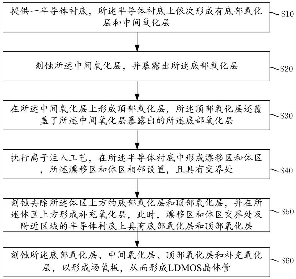
[0046] figure 2 is a schematic flow chart of a method for fabricating an LDMOS transistor in this embodiment. like figure 2 As shown, the preparation method of an LDMOS transistor provided in this embodiment includes the following steps:

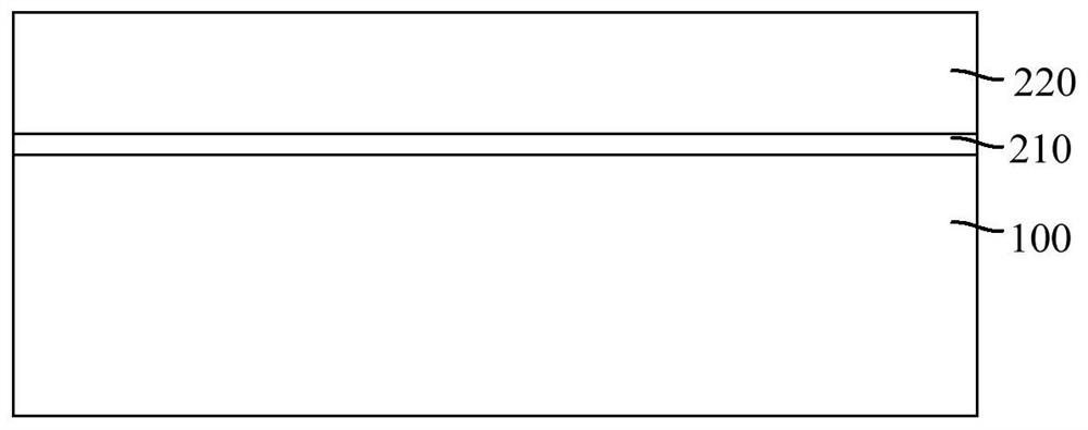
[0047] Step S10: providing a semiconductor substrate, on which a bottom oxide layer and an intermediate oxide layer are sequentially formed;

[0048] Step S20: etching the middle oxide layer, and exposing the bottom oxide layer;

[0049] Step S30: forming a top oxide layer on the middle oxide layer, the top oxide layer also covering the bottom oxide layer exposed by the middle oxide layer;

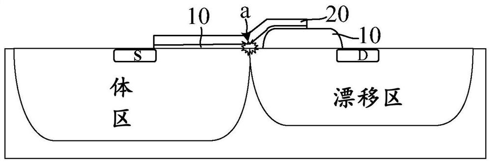
[0050] Step S40: performing an ion implantation process to form a drift region and a body region in the semiconductor substrate, the drift region and the body region are arranged adjacently and have a junction;

[0051]Step S50: removing the bottom oxide layer and the top oxide layer above the body region to expose the semiconductor substrate, and ...


PUM


Abstract

The invention provides an LDMOS transistor and a preparation method thereof, and the preparation method comprises the following steps: providing a semiconductor substrate, and forming a bottom oxide layer and an intermediate oxide layer; etching the intermediate oxide layer; forming a top oxide layer on the intermediate oxide layer; executing an ion implantation process, and forming a drift regionand a body region in the semiconductor substrate; removing the bottom oxide layer and the top oxide layer, forming a supplementary oxide layer above the body region, and forming a bottom oxide layerand a top oxide layer on the semiconductor substrate at the junction of the drift region and the body region and in the vicinity of the junction; and etching the bottom oxide layer, the middle oxide layer, the top oxide layer and the supplementary oxide layer to form the field oxide plate. According to the invention, the bottom oxide layer and the intermediate oxide layer at the junction of the body region and the drift region and in the vicinity of the junction are thicker, so that the overall thickness of the field oxide plate is increased, and when the structure is used, although the electric field at the junction is maximum, the problem of hot carrier injection failure does not occur in the reliability evaluation process.

Description

technical field [0001] The invention relates to the field of semiconductor integrated circuit manufacturing, in particular to an LDMOS transistor and a preparation method thereof. Background technique [0002] The BCD process is a process for fabricating a bipolar junction transistor (Bipolar Junction Transistor, BJT), a complementary metal oxide semiconductor (CMOS), and a diffused metal oxide semiconductor (DMOS) on the same chip. In the process of preparing LDMOS (Laterally Diffused Metal Oxide Semiconductor) transistors using BCD technology, field plates are usually used to reduce the electric field and increase the voltage, such as figure 1 As shown, the field plate is extended from the polysilicon gate 30 to straddle the intermediate oxide layer 10 (Field Oxide, FOX, referred to as Field Oxide). [0003] However, the electric field of this structure is the largest at the junction a of the body region and the drift region, so that the problem of hot carrier injection (...

Claims


Application Information

Patent Timeline
Patent Type & Authority Applications(China)
IPC IPC(8): H01L21/336H01L29/78H01L29/40
CPCH01L29/402H01L29/66681H01L29/7816
Inventor 吴亚贞
Owner SHANGHAI HUAHONG GRACE SEMICON MFG CORP
Why Eureka
Try Eureka