Multi-level inverter circuit and system based on switched capacitor and diode clamping
A multi-level inverter and diode clamping technology, applied to electrical components, output power conversion devices, AC power input conversion to DC power output, etc., can solve the problems of increasing the number of switching tubes and circuit loss
- Summary
- Abstract
- Description
- Claims
- Application Information
AI Technical Summary
Problems solved by technology
Method used
Image
Examples
Embodiment 1
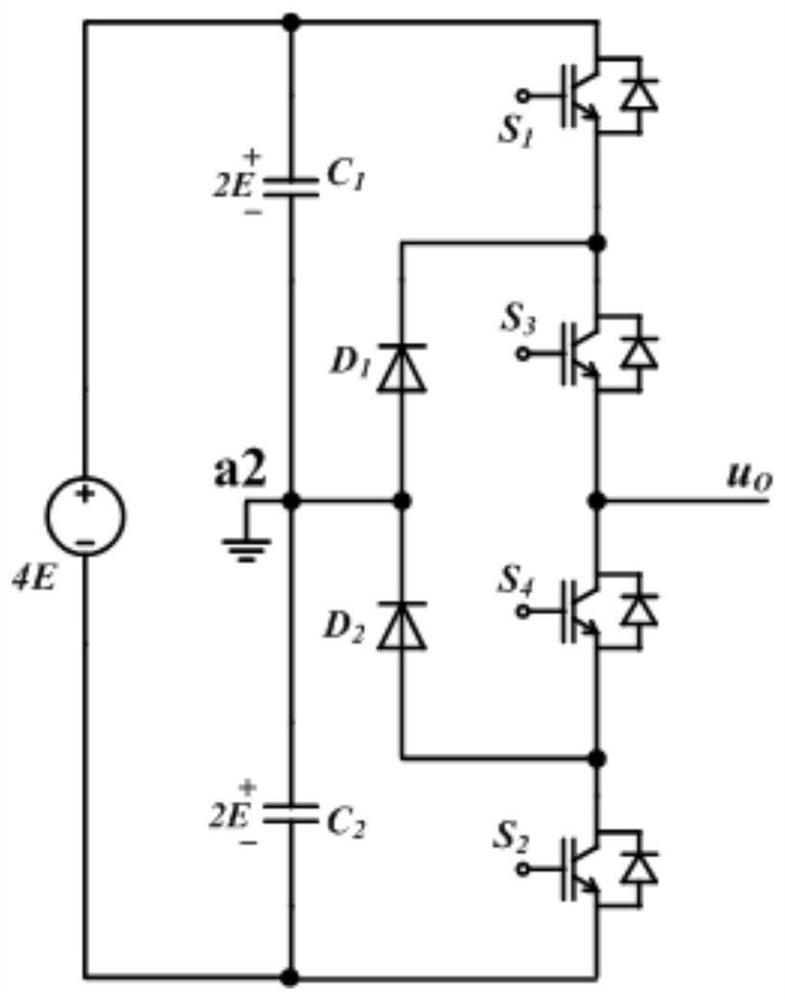
[0060] Such as figure 1 As shown in the traditional typical diode-clamped three-level inverter circuit, the voltage of the DC power supply is +4E, and the circuit consists of four full-control switches S 1 ~S 4 and 2 diodes D 1 ~D 2 , Capacitor C 1 and capacitor C 2 form, capacitor C 1 and capacitor C 2 is the input voltage divider capacitor, normally, the capacitor C 1 and capacitor C 2 Each bears the voltage of +2E, and the capacitor C 1 and capacitor C 2 The connection point a2 of the three-level inverter circuit is the neutral point of the three-level inverter circuit. By controlling the orderly on-off of four full-control switches, the circuit can convert the DC power supply voltage 4E into three levels of 0 and ±2E. AC output, specifically, when the first full-control switch S1 and the third full-control switch S3 are turned on and the second full-control switch S2 and the fourth full-control switch S4 are turned off, the output level is +2E; when the second W...
PUM
 Abstract
Description
Claims
Application Information


