LDMOS and manufacturing method thereof

A manufacturing method and area technology, applied in semiconductor/solid-state device manufacturing, electrical components, circuits, etc., can solve the problems of large on-resistance in the drift region and affecting the performance of LDMOS

Pending Publication Date: 2020-10-27
GTA SEMICON CO LTD
View PDF6 Cites 0 Cited by
  • Summary
  • Abstract
  • Description
  • Claims
  • Application Information

AI Technical Summary

Problems solved by technology

In this LDMOS, the doping concentration and depth of the drift region are limited and the requirements for breakdown of the CMOS (complementary metal oxide semiconductor) we

Method used


Image

  • LDMOS and manufacturing method thereof
  • LDMOS and manufacturing method thereof
  • LDMOS and manufacturing method thereof

Examples


Embodiment 1

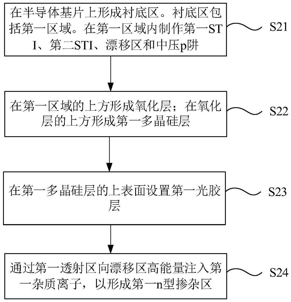
[0050] This embodiment provides a manufacturing method of LDMOS, referring to Figure 2 to Figure 9 , the production method includes the following steps:

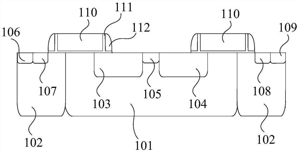
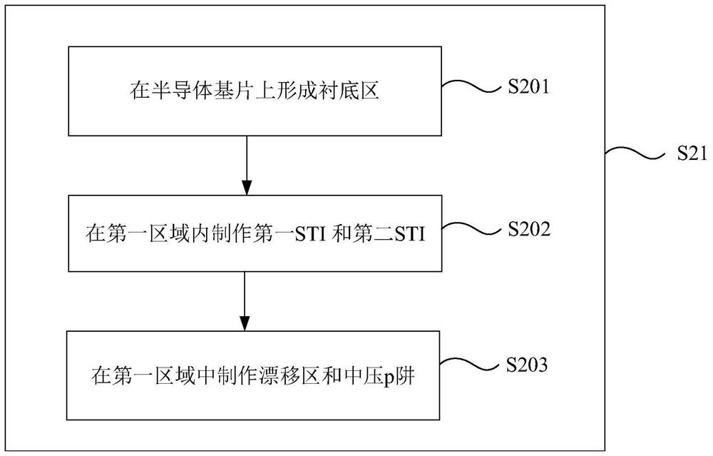
[0051] Step S21 , forming a substrate region on the semiconductor substrate. The substrate region comprises a first region 11 . The first STI 103, the second STI 104, the drift region 101 and the medium voltage p-well 102 are fabricated in the first region.

[0052] As a preferred implementation manner, step S1 includes:

[0053] Step S201, forming a substrate region on a semiconductor substrate.

[0054] Step S202 , making the first STI 103 and the second STI 104 in the first area 11 . Make a state reference after forming the first STI 103 and the second STI 104 Figure 4 .

[0055] Step S203 , fabricating a drift region 101 and a medium voltage p-well 102 in the first region 11 . The depth of the drift region 101 is greater than the depths of the first STI 103 and the second STI 104 . State reference after fabrica...

Embodiment 2

[0064] On the basis of the manufacturing method of the LDMOS in the first embodiment, this embodiment provides a manufacturing method of the LDMOS, the LDMOS further includes a high-resistance device, and the high-resistance device is formed by using the second region of the substrate region.

[0065] The flow process of making LDMOS by adopting the manufacturing method of LDMOS of the present embodiment is as follows:

[0066] In step S21, first, a substrate region is formed on a semiconductor substrate. refer to Figure 10 , the substrate region includes a first region 11 and a second region 12 . The first STI 103 and the second STI 104 are fabricated in the first region 11 , while the third STI 121 is fabricated in the second region 12 .

[0067] Then, refer to Figure 11 , and simultaneously implant the same impurity ions into the first region 11 and the second region 12 to form the drift region 101 in the first region 11 and form the first doped region 122 in the secon...


PUM


Abstract

The invention discloses an LDMOS and a manufacturing method thereof. The manufacturing method comprises the following steps: forming a substrate region on a semiconductor substrate, wherein the substrate region comprises a first region; manufacturing a first STI, a second STI, a drift region and a medium-voltage p well in the first region; forming an oxide layer above the first region; forming a first polycrystalline silicon layer above the oxide layer; arranging a first optical cement layer on the upper surface of the first polycrystalline silicon layer, wherein the first optical cement layercomprises a first transmission region and a first blocking region, and the first blocking region is used for blocking foreign ions from passing through; and injecting first impurity ions into the drift region at high energy through the first transmission region to form a first n-type doped region. According to the invention, impurity ions are injected into the drift region of the LDMOS at high energy, so that the on resistance of the drift region is reduced, and the breakdown voltage can be maintained.

Description

technical field [0001] The invention belongs to the technical field of LDMOS (Lateral Diffusion Gate Transistor) production, and in particular relates to an LDMOS and a production method thereof. Background technique [0002] State-of-the-art LDMOS such as figure 1 As shown, it includes a drift region (n-type) 101, a medium-voltage p-well 102, a first STI (shallow trench isolation) 103, a second STI (shallow trench isolation) 104, a first n-type heavily doped region 105, The second n-type heavily doped region 107, the third n-type heavily doped region 109, the first p-type heavily doped region 106, the second n-type heavily doped region 108, the gate 110, the oxide layer 111, the metal electrode 112. In this LDMOS, the doping concentration and depth of the drift region are limited and the requirements for breakdown of the CMOS (complementary metal oxide semiconductor) well cannot be flexibly changed according to the requirements of the device, and the on-resistance of the ...

Claims


Application Information

Patent Timeline
IPC IPC(8): H01L21/336H01L29/78
CPCH01L29/66689H01L29/7816
Inventor 林威
Owner GTA SEMICON CO LTD
Why Eureka
Try Eureka