
Backside illuminated image sensor and manufacturing method thereof

A technology of an image sensor and a manufacturing method, which is applied to semiconductor devices, electric solid-state devices, radiation control devices, etc., can solve the problems of poor pattern alignment accuracy, easy changes in the engraving accuracy of the ground layer 130, affecting process efficiency, etc.

Active Publication Date: 2020-10-27
SHANGHAI HUALI MICROELECTRONICS CORP
View PDF4 Cites 0 Cited by
  • Summary
  • Abstract
  • Description
  • Claims
  • Application Information

AI Technical Summary

Problems solved by technology

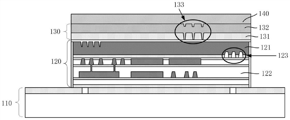
However, in the manufacturing process of the back-illuminated image sensor, the overlay accuracy of the ground layer 130 is likely to change, resulting in the patterned grating isolation layer 140 and the pattern in the device wafer 120 using the ground mark structure 133 as an alignment reference. Alignment accuracy is poor
In order to improve the alignment accuracy of the grating isolation layer and the pattern in the device wafer, engineers usually need to update the compensation value of the overlay accuracy of the grating isolation layer according to the change of the overlay accuracy of the ground layer, which affects the process efficiency

Method used


Image

  • Backside illuminated image sensor and manufacturing method thereof
  • Backside illuminated image sensor and manufacturing method thereof
  • Backside illuminated image sensor and manufacturing method thereof

Examples


Embodiment Construction

[0030] The back-illuminated image sensor proposed by the present invention and its manufacturing method will be further described in detail below with reference to the accompanying drawings and specific embodiments. The advantages and features of the present invention will become clearer from the following description. It should be noted that all the drawings are in a very simplified form and use imprecise scales, and are only used to facilitate and clearly assist the purpose of illustrating the embodiments of the present invention.

[0031] refer to figure 1 , as mentioned in the background art, in the traditional manufacturing method of the back-illuminated image sensor, after the ground layer 130 is formed, it is also necessary to form, for example, a patterned grating isolation layer 140 on the ground layer 130 . Since the ground layer 130 includes a metal material layer 132, laser light and the like cannot penetrate the metal material layer 132 in the subsequent photolit...


PUM


Abstract

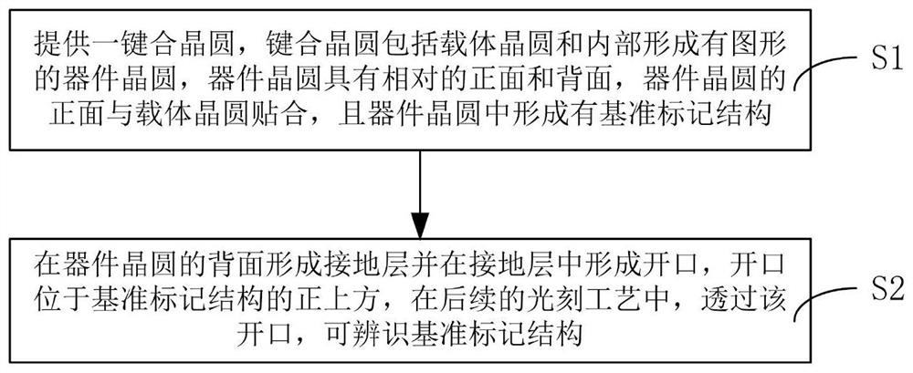
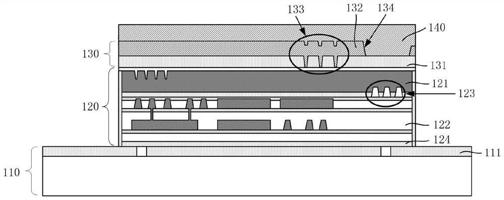
The invention provides a backside illuminated image sensor and a manufacturing method thereof. The manufacturing method comprises the steps that a bonding wafer comprising a carrier wafer and a devicewafer is provided, the front face of the device wafer is attached to the carrier wafer, and a reference mark structure is formed in the device wafer; a grounding layer is formed on the back surface of the device wafer and an opening is formed in the grounding layer, the opening is positioned right above the reference mark structure; in a subsequent photoetching process, the reference mark structure can be identified through the opening, so that the patterned functional layer formed on the grounding layer subsequently can take the reference mark structure as an alignment reference, the alignment precision of the functional layer and a graph in a device wafer can be improved, and the performance of the backside illuminated image sensor is improved. The invention also provides the backside illuminated image sensor manufactured by using the manufacturing method of the backside illuminated image sensor.

Description

technical field [0001] The invention relates to the technical field of semiconductors, in particular to a back-illuminated image sensor and a manufacturing method thereof. Background technique [0002] figure 1 It is a schematic cross-sectional view of an existing back-illuminated image sensor. refer to figure 1 , in the manufacturing process of the back-illuminated image sensor (BSI), the following steps are included: a) bonding the front surface of the device wafer 120 with a pattern formed inside to the carrier wafer 110 to form a bonded wafer; b) A ground layer 130 is formed on the back side of the device wafer 120, the ground layer 130 includes a dielectric layer 131 and a metal material layer 132 (such as an aluminum metal layer), and a ground mark structure 133 is formed on the ground layer 130; c) on the ground layer 130 The grating isolation layer 140 is formed, and the grating isolation layer 140 is patterned. [0003] During the above-mentioned patterning proc...

Claims


Application Information

Patent Timeline
IPC IPC(8): H01L27/146H01L23/544
CPCH01L27/1464H01L27/14683H01L23/544
Inventor 何洪波王剑
Owner SHANGHAI HUALI MICROELECTRONICS CORP
Learn More