Supercharge Your Innovation With Domain-Expert AI Agents!

Charge pump circuit, chip and electronic equipment

A charge pump and circuit technology, applied in the field of circuits, can solve the problems of the chip cannot meet the requirements of the application side, the duration is short, and the performance of electronic equipment is reduced.

Pending Publication Date: 2020-10-27
SHENZHEN GOODIX TECH CO LTD
View PDF7 Cites 0 Cited by
  • Summary
  • Abstract
  • Description
  • Claims
  • Application Information

AI Technical Summary

Problems solved by technology

The flying capacitor or output capacitor in the charge pump circuit will generate a peak transient current with a duration as short as a few nanoseconds (ns) and an amplitude as high as hundreds of milliamperes (mA) during the charging or discharging process. The electromagnetic field and electromagnetic waves generated by the current will interfere with other circuit modules near the chip, especially the antenna that is extremely sensitive to Electromagnetic Interference (EMI), which will greatly reduce the performance of electronic equipment, so that the designed chip cannot meet the requirements of the application side.

Method used


Image

  • Charge pump circuit, chip and electronic equipment
  • Charge pump circuit, chip and electronic equipment
  • Charge pump circuit, chip and electronic equipment

Examples


Embodiment Construction

[0050] The technical solution in this application will be described below with reference to the accompanying drawings.

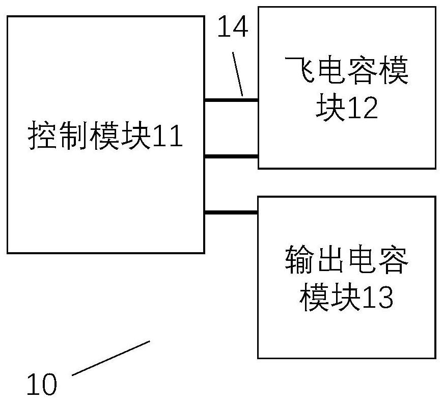
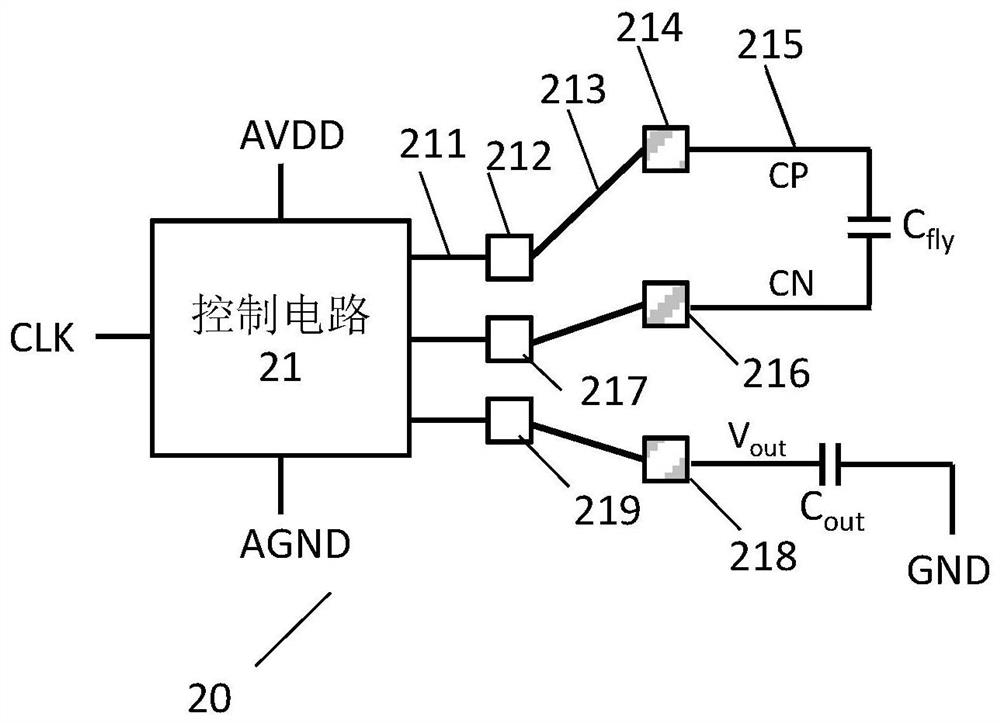
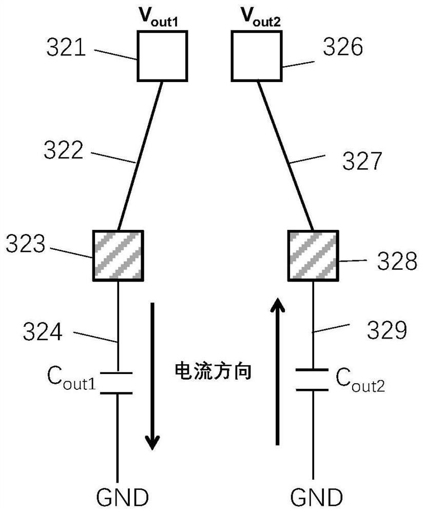
[0051]The flying capacitor Cfly and the output capacitor Cout in the charge pump circuit are periodically charged and discharged to obtain a stable boosted or bucked output voltage Vout. According to the working principle of the charge pump circuit, the two ends of the flying capacitor Cfly are generally divided into CP and CN. The CP is the end connected to the positive plate of the flying capacitor, and the CN is the end connected to the negative plate of the flying capacitor. In the charging state, the current flows from the CP terminal through the flying capacitor Cfly to the CN terminal. When the flying capacitor Cfly is in the discharging state, that is, when the flying capacitor Cfly charges the output capacitor Cout, the current flows from the CN terminal through the flying capacitor Cfly to the CP terminal. The non-ground terminal of the output capa...


PUM


Abstract

The invention discloses a charge pump circuit, a touch chip and electronic equipment. The charge pump circuit comprises a first charge pump module and a second charge pump module. The first charge pump module comprises a first control module, a first output capacitor (Cout1) and a fourth bonding pad (321); the second charge pump module comprises a second control module, a second output capacitor and a fifth bonding pad (326). When the first output capacitor (Cout1) is in a charging state, the second output capacitor (Cout2) is in a discharging state; or when the first output capacitor (Cout1)is in a discharging state and the second output capacitor (Cout2) is in a charging state, the fourth bonding pad (321) and the fifth bonding pad (326) are arranged adjacent to each other. Or when thefirst output capacitor (Cout1) is in the charging state, the second output capacitor (Cout2) is in the charging state; or when the first output capacitor (Cout1) is in a discharge state and the secondoutput capacitor (Cout2) is in a discharge state, a grounding module is placed between the fourth bonding pad (321) and the fifth bonding pad (326). According to the circuit structure, electromagnetic interference is reduced, and the performance of the chip is improved.

Description

technical field [0001] The embodiments of the present application relate to the circuit field, and in particular, to a charge pump circuit, a chip, and an electronic device. Background technique [0002] Currently, integrated circuit chips usually use a charge pump (charge pump) circuit for step-up or step-down processing. The flying capacitor or output capacitor in the charge pump circuit will generate a peak transient current with a duration as short as a few nanoseconds (ns) and an amplitude as high as hundreds of milliamperes (mA) during the charging or discharging process. The electromagnetic field and electromagnetic waves generated by the current will interfere with other circuit modules near the chip, especially the antenna that is extremely sensitive to Electromagnetic Interference (EMI), which will greatly reduce the performance of electronic equipment, so that the designed chip cannot meet the requirements of the application side. . Contents of the invention ...

Claims


Application Information

Patent Timeline
IPC IPC(8): H02M3/07H02M1/44
CPCH02M3/07H02M1/44
Inventor 刘诗雨
Owner SHENZHEN GOODIX TECH CO LTD
Features
  • R&D
  • Intellectual Property
  • Life Sciences
  • Materials
  • Tech Scout
  • Unparalleled Data Quality
  • Higher Quality Content
  • 60% Fewer Hallucinations
Learn More