Chip encapsulation testing method and device

A chip mounting and chip technology, which is applied in the field of chip packaging and testing methods and devices, and can solve problems such as the position deviation of the suction nozzle relative to the chip

Inactive Publication Date: 2020-10-30
CHONGQING UNIV OF ARTS & SCI
View PDF0 Cites 0 Cited by
  • Summary
  • Abstract
  • Description
  • Claims
  • Application Information

AI Technical Summary

Problems solved by technology

[0004] One of the objectives of the present invention is to provide a chip packaging and testing method to solve the problem that in the current chip packaging and testing process, when the separation device is used to separate the chip from the blue film, the chip will move upward under the suction of the suction nozzle. Drive the blue film to move up, resulting in the problem that the position of the nozzle relative to the chip will deviate in the next separation operation

Method used


Image

  • Chip encapsulation testing method and device
  • Chip encapsulation testing method and device
  • Chip encapsulation testing method and device

Examples


Embodiment Construction

[0036] The following is further described in detail through specific implementation methods:

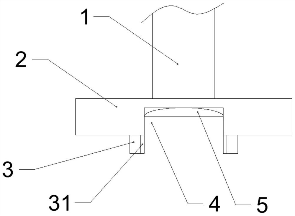
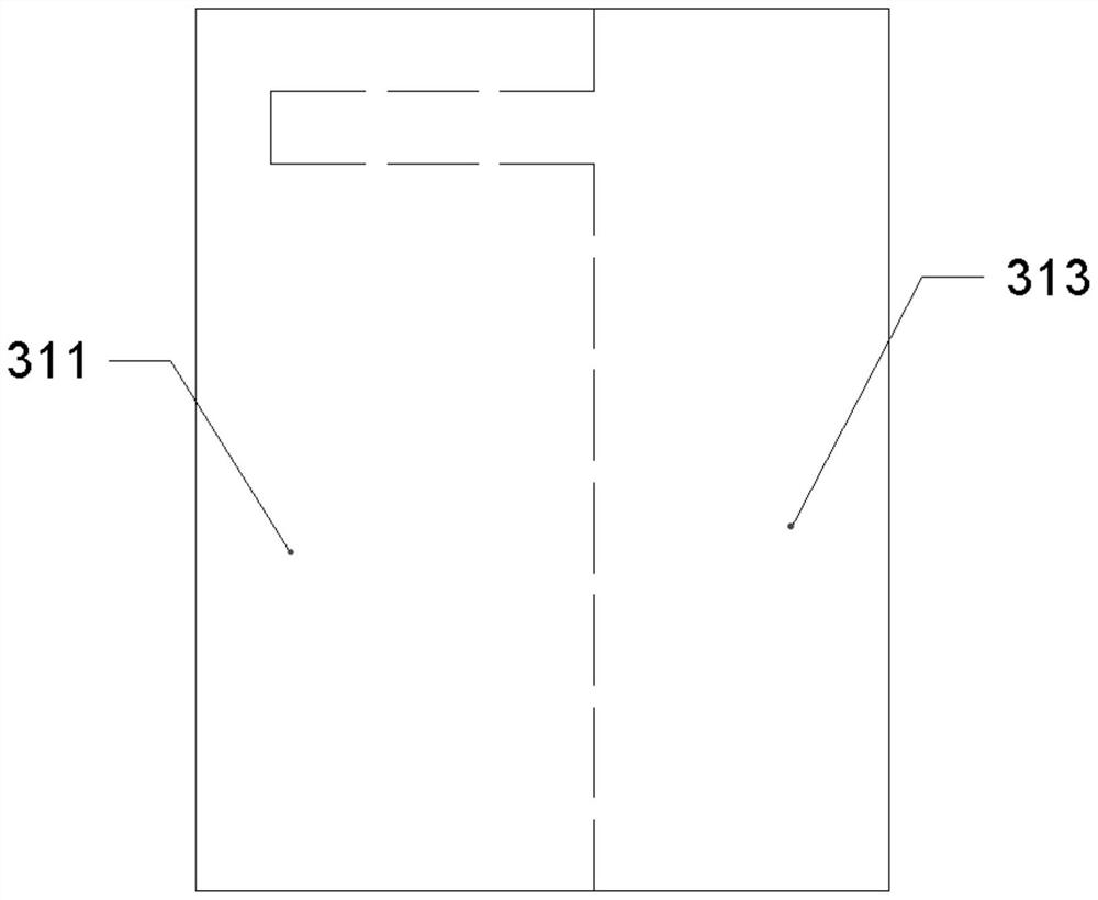
[0037]The reference numerals in the accompanying drawings of the description include: the driving rod 1 , the pick-up plate 2 , the pressing block 3 , the connecting block 31 , the first pressing portion 311 , the second pressing portion 313 , the inner concave portion 4 , and the suction nozzle 5 .

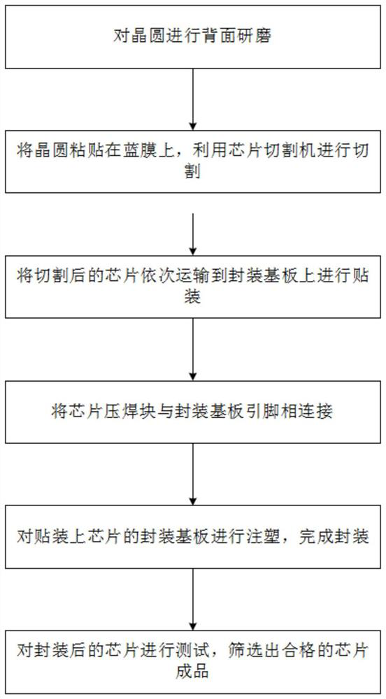
[0038] The embodiment is basically as attached Figure 1 to Figure 3 Shown: a chip packaging and testing method, including the following steps: Wafer thinning step: back grinding the wafer;

[0039] Wafer cutting step: Paste the wafer on the blue film, and cut the wafer with a chip cutting machine;

[0040] Chip mounting step: the pick-up board 2 with the suction nozzle 5 moves according to the preset movement route, and the cut chips are sequentially transported to the packaging substrate for mounting;

[0041] Specifically, the chip mounting step includes the following steps:

[00...


PUM


Abstract

The invention relates to the technical field of chip packaging and aims to solve a problem that, in a chip packaging and testing process, when a separation device is used for realizing the separationof a chip and a blue film, when the chip moves upwards, the blue film is driven to move upwards. The chip packaging and testing method comprises a wafer thinning step, a wafer cutting step, a chip mounting step, a chip interconnection step, a forming step and a testing step, and is characterized in that the chip mounting step comprises the following steps that a pickup plate descends so that a suction nozzle on the pickup plate abuts against a to-be-packaged chip, and pressing blocks located at two ends of the suction nozzle press chips at two ends of the to-be-packaged chip at the same time;after the suction nozzle sucks the chip to be packaged, the pickup plate moves upwards and moves to a position above a corresponding mounting position on the packaging substrate; and S4, the pickup plate descends, the to-be-packaged chip is in contact with the mounting position, and meanwhile, the pressing blocks press the chips mounted at two ends of the mounting position.

Description

technical field [0001] The invention relates to the technical field of chip packaging, in particular to a chip packaging and testing method and device. Background technique [0002] Chip packaging and testing refers to the process of processing the tested wafers into independent chips according to the product model and functional requirements. The existing chip packaging and testing process includes chip packaging and post-packaging testing steps. In chip packaging, the existing packaging The basic process of the process is: wafer thinning - wafer cutting - chip mounting - chip interconnection - forming technology, etc. Among them, after the thinned wafer is pasted on the blue film during wafer cutting, it is sent to the chip cutting machine for cutting. During the cutting process, the wafer is cut into multiple chips, and the blue film is set. Ensure that multiple chips after cutting will not be scattered, and play a role in fixing the position of the chip. Therefore, in ...

Claims


Application Information

Patent Timeline
Patent Type & Authority Applications(China)
IPC IPC(8): H01L21/67H01L21/683
CPCH01L21/67132H01L21/67253H01L21/67271H01L21/6836H01L21/6838H01L2221/68327
Inventor 李强康阳黄羿
Owner CHONGQING UNIV OF ARTS & SCI
Why Eureka
Try Eureka