
Optical synapse device based on amorphous silicon thin film, preparation method and working method

A technology of amorphous silicon thin film and amorphous silicon, which is applied in the direction of semiconductor devices, sustainable manufacturing/processing, electrical components, etc., can solve the problems of working bandwidth limitation, inability to distinguish excitation light wavelengths, etc., and achieve simple device structure and preparation process , Solve the effect of limited working bandwidth

Active Publication Date: 2022-04-22
UNIV OF ELECTRONICS SCI & TECH OF CHINA
View PDF6 Cites 0 Cited by
  • Summary
  • Abstract
  • Description
  • Claims
  • Application Information

AI Technical Summary

Problems solved by technology

[0003] Most of the existing patents are synapses with electrical signals as the excitation source (called electrical synapses). This type of synapse device only uses electrical signals as the excitation signal of synapses to realize the function of artificial synapses. Its operating bandwidth is greatly limited
At present, only a few published patents use light as an artificial synapse as an excitation signal (publication numbers: CN109659436A, CN109460819A). This type of optical synapse can respond to light sources of different wavelengths, but cannot distinguish the wavelength of excitation light

Method used


Image

  • Optical synapse device based on amorphous silicon thin film, preparation method and working method
  • Optical synapse device based on amorphous silicon thin film, preparation method and working method
  • Optical synapse device based on amorphous silicon thin film, preparation method and working method

Examples


Embodiment Construction

[0024] Embodiments of the present invention are described below through specific examples, and those skilled in the art can easily understand other advantages and effects of the present invention from the content disclosed in this specification. The present invention can also be implemented or applied through other different specific implementation modes, and various modifications or changes can be made to the details in this specification based on different viewpoints and applications without departing from the spirit of the present invention.

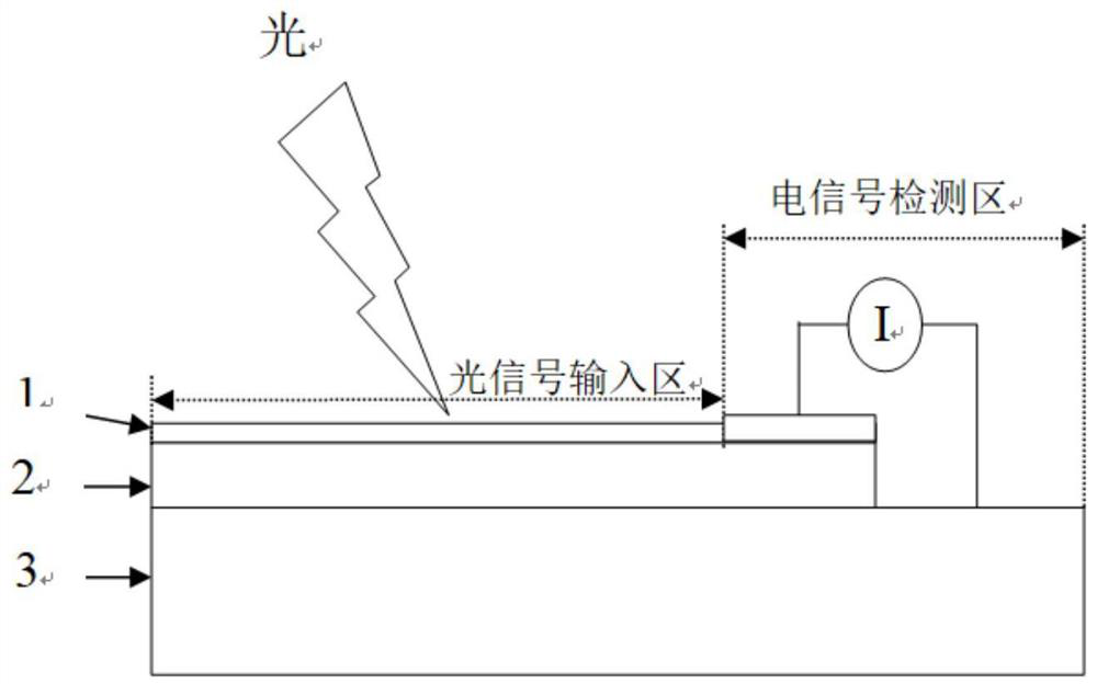
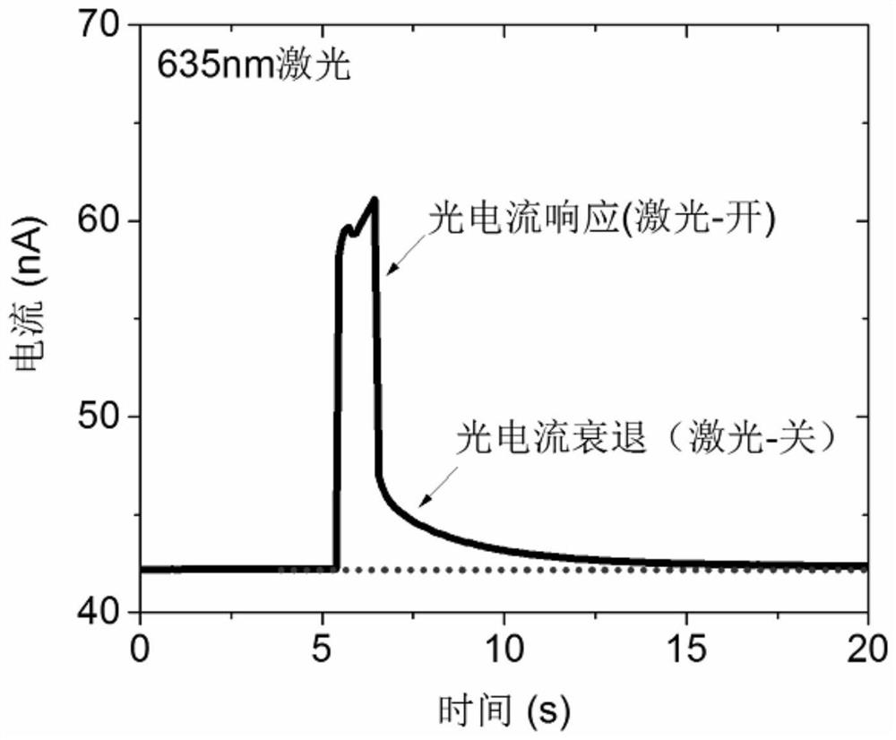
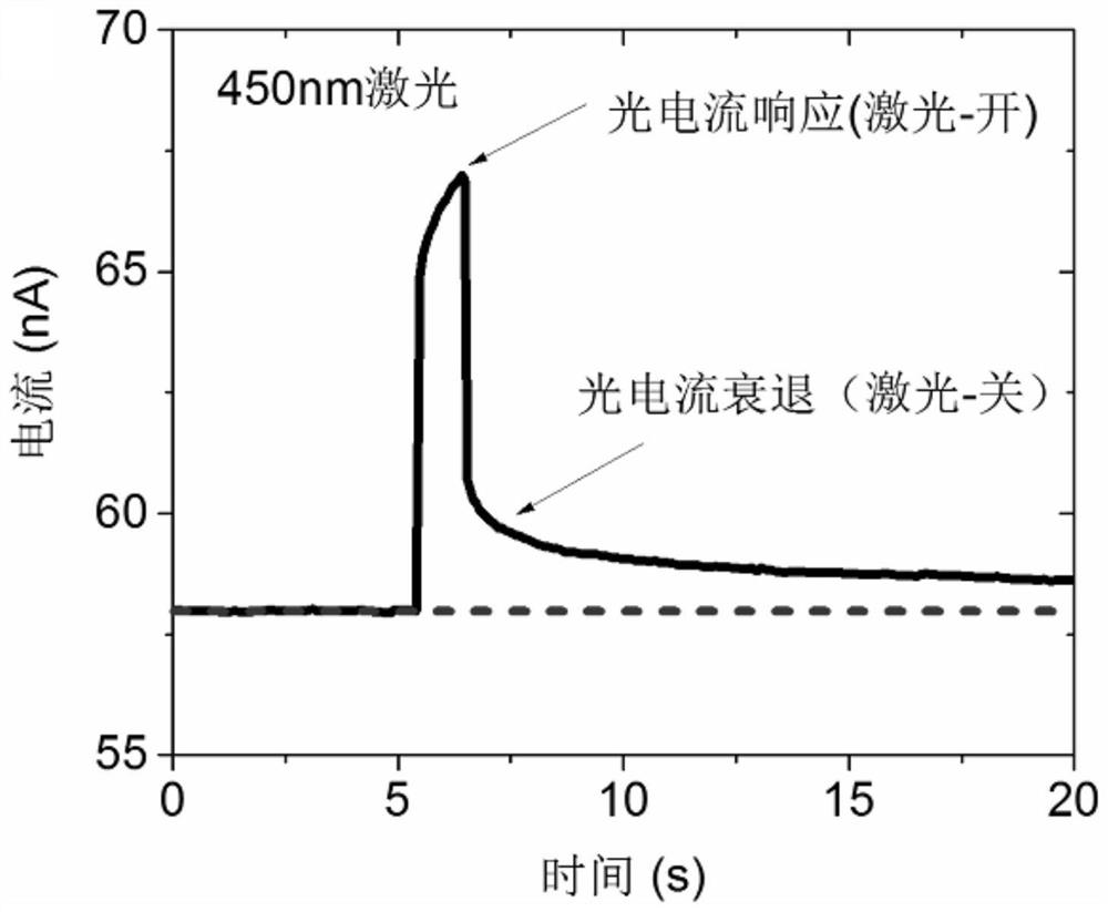
[0025] This embodiment provides an optical synapse device based on an amorphous silicon thin film. The device uses optical signals of different energies as excitation sources, uses optical signals of different energies to simulate the action potential of the front end of the synapse, and uses the photocurrent response of the device to simulate The post-synaptic current realizes the bionic synapse function with color recognition ability...


PUM

PropertyMeasurementUnit
thicknessaaaaaaaaaa
thicknessaaaaaaaaaa
surface roughnessaaaaaaaaaa

Abstract

The invention provides an optical synapse device and method based on an amorphous silicon thin film. The device uses optical signals of different energies as excitation sources, and uses optical signals of different energies to simulate the action potential of the front end of the synapse. Selectively excite photo-generated carriers, use the defect energy level in the amorphous silicon film to capture and release photo-generated carriers to cause changes in photocurrent, and use the photocurrent response of the device to simulate post-synaptic currents to achieve different colors. The recognition of energy, thus the bionic synapse function with color selective recognition ability, skillfully utilizes the change of the photocurrent response of the defect energy level represented by the dangling bond in the amorphous silicon film to the capture and release of photogenerated carriers, To realize the synaptic function of the device, the photoelectric synapse of the present invention not only has the characteristics of simple device structure and preparation process and is compatible with the Si-CMOS process, but also has the ability of color recognition, which can solve the limited working bandwidth of the electro-stimulated electrical reading synapse device The problem.

Description

technical field [0001] The invention belongs to the field of silicon-based photonic integrated devices and neuromorphic chips, and in particular relates to an optical synapse device based on an amorphous silicon film, a preparation method and a working method thereof. Background technique [0002] With the vigorous development of emerging fields such as artificial intelligence, the Internet of Things, and "big data", computers based on Vonno-Iman's architecture are facing severe challenges in terms of size, data processing capabilities, and energy consumption. In order to meet this challenge, the researchers proposed a new type of computer architecture, which uses neuromorphic chips to break through the bottleneck faced by the von Neumann architecture. Neuromorphic chips, also commonly referred to as "brain-like chips," consist of "neurons" and "synapses" that connect two different neurons. In the neuromorphic chip, the synaptic unit can realize the integrated function of c...

Claims


Application Information

Patent Timeline
Patent Type & Authority Patents(China)
IPC IPC(8): H01L31/0376H01L31/20G06N3/067
CPCH01L31/03762H01L31/03767H01L31/202G06N3/067Y02P70/50
Inventor 李伟田伟陈鹏宇伊海李东阳李春梅蒋向东
Owner UNIV OF ELECTRONICS SCI & TECH OF CHINA
Learn More