

Synaptic transistor and preparation method thereof
A transistor and synapse technology, applied in the field of synaptic transistors and their preparation, can solve the problems of unstable physical and chemical properties of organic channel materials, unfavorable device stability and subsequent integration, and increase the difficulty of large-scale integration. Application and large-scale integration, good application value, the effect of reducing the difficulty of preparation
- Summary
- Abstract
- Description
- Claims
- Application Information
AI Technical Summary
Problems solved by technology
Method used
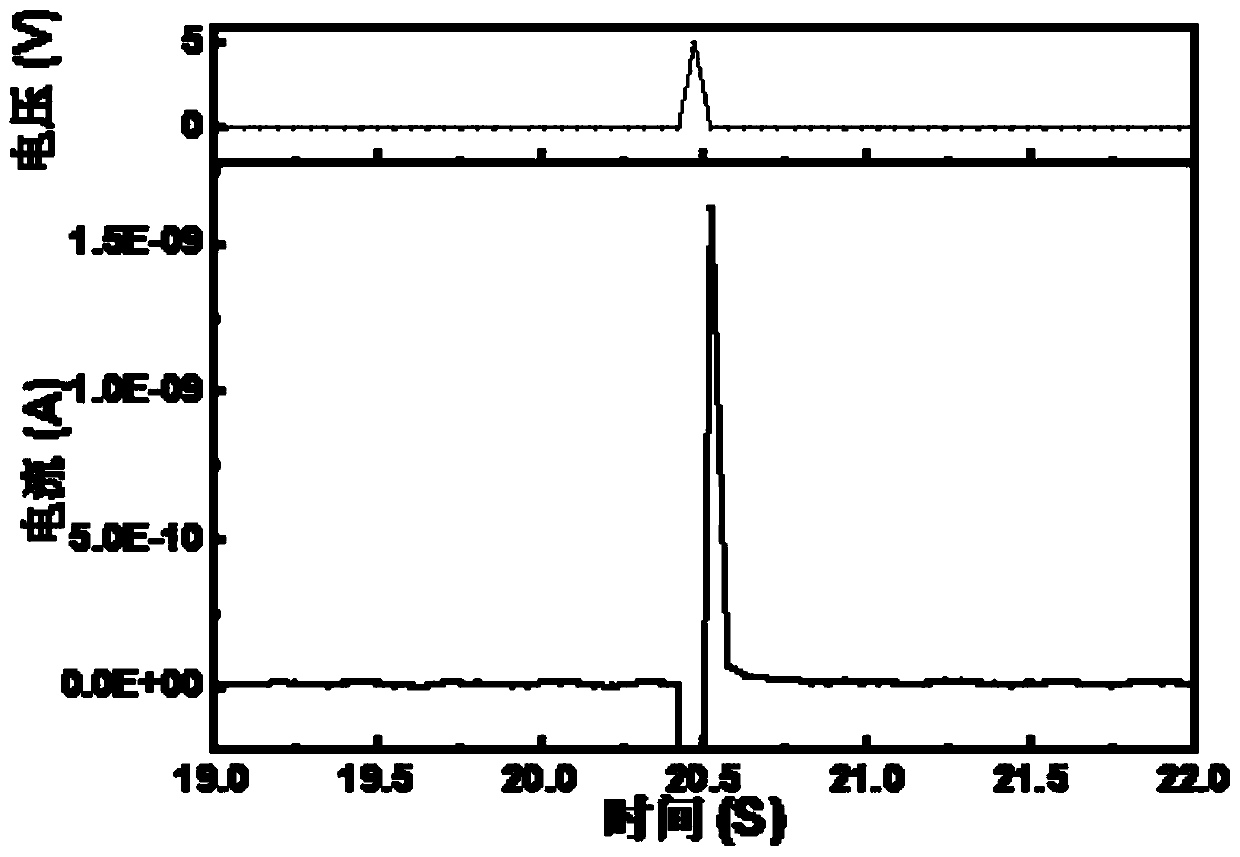
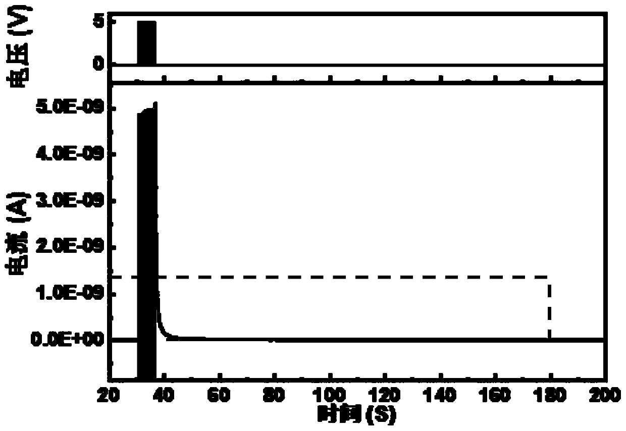
Image

Examples
Embodiment 1
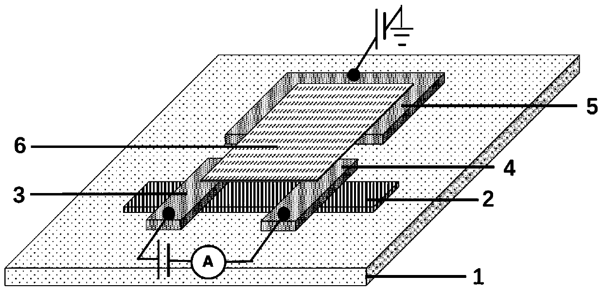
[0038] In this embodiment, the device structure is as figure 1 As shown, an insulating substrate 1 and a channel material 2, a source electrode 3, a drain electrode 4, and a gate electrode 5 on the substrate 1 are included to form a planar three-terminal synaptic transistor. The source electrode 3 and the drain electrode 4 are respectively located at two ends of the channel material 2 and form an ohmic contact with the channel material 2. A solid electrolyte 6 is covered on the channel region and part of the gate electrode region, and the solid electrolyte 6 contains an organic carrier that is electrically insulated and movable ions.
[0039] In this embodiment, the substrate is a silicon wafer with a surface silicon dioxide layer, and the thickness of the silicon dioxide layer is 300 nm. The channel material is tetrahedral amorphous carbon (Tac). The source electrode 3, the drain electrode 4, and the gate electrode 5 all use Pt / Ti. The solid electrolyte contains polyethylene o...
PUM
| Property | Measurement | Unit |
|---|---|---|
| thickness | aaaaa | aaaaa |
| electrical resistivity | aaaaa | aaaaa |
| dielectric strength | aaaaa | aaaaa |
Abstract
Description
Claims
Application Information