
Inverted light emitting diode with embedded scattering layer and preparation method thereof

A technology of light-emitting diodes and scattering layers, which is applied to semiconductor devices, electrical components, circuits, etc., can solve the problems of low light emission efficiency of LEDs and low photon escape probability, and achieve increased photon escape probability, shortened propagation path, and improved The effect of light extraction efficiency

Active Publication Date: 2020-10-30
贵溪穿越光电科技有限公司
View PDF17 Cites 1 Cited by
  • Summary
  • Abstract
  • Description
  • Claims
  • Application Information

AI Technical Summary

Problems solved by technology

However, the light emitted by the active region will be consumed by repeated reflections between the bottom reflective layer and the cavity of the sapphire substrate, making the probability of photon escape low, and the LED light output efficiency is not high

Method used


Image

  • Inverted light emitting diode with embedded scattering layer and preparation method thereof

Examples


Embodiment Construction

[0031] In order to make the object, technical solution and advantages of the present invention clearer, the present invention will be further described in detail below in conjunction with the accompanying drawings. It should be understood that the specific embodiments described here are only used to explain the present invention, not to limit the present invention.

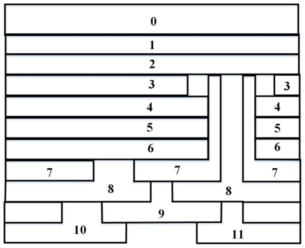
[0032] The technical solution provided by the embodiment of the present invention is: a flip-chip light-emitting diode with an embedded scattering layer, such as figure 1 As shown, it includes a sapphire substrate 0, on which a u-GaN layer 1, an n-GaN layer 2, an n+-GaN layer 3, a light-emitting layer 4 and a p-GaN layer 5 are sequentially grown; the p - A transparent conductive layer 6 is deposited on the GaN layer 5; the transparent conductive layer 6, p-GaN layer 5, light emitting layer 4 and n+-GaN layer 3 are etched with three-dimensional n-type through holes directly reaching the p-GaN layer 5 array; and et...


PUM

PropertyMeasurementUnit
thicknessaaaaaaaaaa

Abstract

The invention discloses an inverted light emitting diode with an embedded scattering layer, the inverted light emitting diode comprises a sapphire substrate, and a u-GaN layer, an n-type doped nitridematerial layer, a heavily doped n-type doped nitride material layer, a light emitting layer and a p-type doped nitride material layer are sequentially grown on the sapphire substrate. A transparent conductive layer is deposited on the p-type doped nitride material layer; a three-dimensional n-type through hole array directly reaching the p-type doped nitride material layer is etched on the transparent conductive layer, the p-type doped nitride material layer, the light emitting layer and the heavily doped n-type doped nitride material layer; an air gap structure communicated with the three-dimensional n-type through hole array is etched on the heavily doped n-type doped nitride material layer; bottom reflecting layers are deposited on the transparent conductive layer and in the three-dimensional n-type through hole array, and electrodes are arranged on the bottom reflecting layers. An air gap structure array is formed on the sapphire substrate to form an embedded light scattering layer, so that photons are scattered, the escape probability of the photons is increased, and the light emitting efficiency of the LED is improved.

Description

technical field [0001] The invention relates to the technical field of semiconductor light-emitting diodes, in particular, the invention relates to a flip-chip light-emitting diode with an embedded scattering layer and a preparation method thereof. Background technique [0002] In the prior art, the flip-chip structure LED chip is bonded on the substrate with good thermal conductivity, and the direction of the electrode is downward, so that the heat is transferred to the substrate, the heat dissipation effect is greatly improved, and the light emitted to the bottom is reflected upwards. The light is emitted from the sapphire substrate with high transmittance, and the light extraction efficiency is improved. However, the light emitted by the active region will be consumed by repeated reflections between the bottom reflective layer and the cavity of the sapphire substrate, so that the probability of photon escape is low, and the light output efficiency of the LED is not high. ...

Claims


Application Information

Patent Timeline
Patent Type & Authority Applications(China)
IPC IPC(8): H01L33/10H01L33/32H01L33/36H01L33/00
CPCH01L33/0066H01L33/0075H01L33/10H01L33/32H01L33/36
Inventor 周圣君赵杰
Owner 贵溪穿越光电科技有限公司
Learn More