Manufacturing process of acoustic resonator and acoustic resonator

A technology of acoustic wave resonator and manufacturing process, which is applied in the manufacturing process of acoustic wave resonators and the field of acoustic wave resonators, and can solve the problems of unstable filter passband waveform, poor mechanical stability, and affecting the frequency response of resonators, etc.

Active Publication Date: 2020-10-30
HANGZHOU XINGHE TECH CO LTD
View PDF5 Cites 1 Cited by
  • Summary
  • Abstract
  • Description
  • Claims
  • Application Information

AI Technical Summary

Problems solved by technology

[0006] In view of the poor mechanical stability of the existing resonators mentioned above, it is easy to generate parasitic oscillations, affect the freq...

Method used


Image

  • Manufacturing process of acoustic resonator and acoustic resonator
  • Manufacturing process of acoustic resonator and acoustic resonator
  • Manufacturing process of acoustic resonator and acoustic resonator

Examples


Embodiment 1

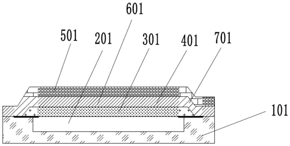
[0040] Such as Figure 3h As shown, the amorphous portion 711 in this embodiment includes the bottom electrode layer 311 , the piezoelectric layer 411 and the top electrode layer 511 sequentially stacked on a part of the resonant film layer 611 perpendicular to the surface of the substrate 111 . Therefore, the amorphous shape of the resonant thin film layer 611 can be realized in the selected partial area of ​​the device, and the amorphous shape of the resonant thin film layer 611 with any pattern on the partial area can be realized.

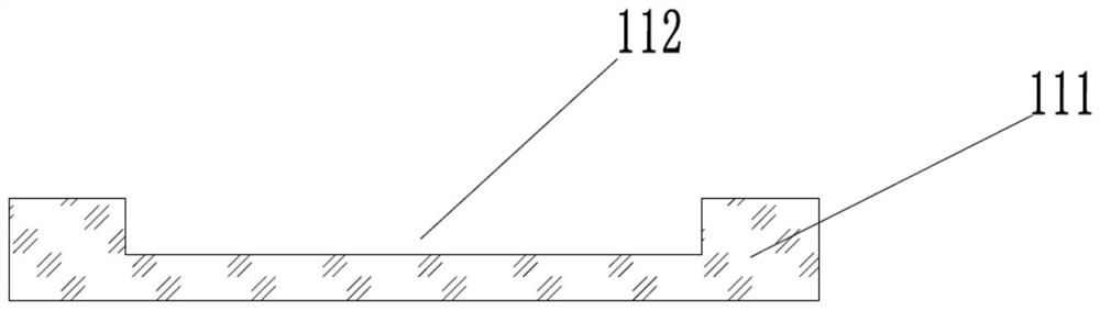
[0041] In a specific embodiment, the substrate 111 corresponding to the amorphous portion 711 is treated to have a rough surface. One side of the rough surface is located within the projection area or coincides with the boundary of the projection area, and the other side is located outside the projection area. A film layer with an amorphous morphology grows on a rough surface. In a preferred embodiment, the roughness is 100A-2000A. The film l...

Embodiment 2

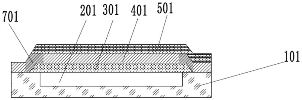
[0050] Such as Figure 5h As shown, the amorphous part 721 in this embodiment is a part of the piezoelectric layer 421 in the resonant film layer 621 . In one of the specific embodiments, the amorphous part 721 is that one side of the projection of the piezoelectric layer 421 on the substrate 121 in the resonant film layer 621 is located within the projection area or coincides with the boundary of the projection area, and the other side is The entire part or a partial part located outside the projected area, the partial part may be a part extending downward from the upper surface of the piezoelectric layer 421 . The piezoelectric layer 421 with an amorphous form weakens the sound velocity of the transverse sound wave to a certain extent, forming a region with a sudden change in acoustic impedance and reflecting the transverse wave.

[0051] In a particular embodiment, the amorphous portion 721 is subjected to a rapid thermal annealing process to have amorphous properties. Th...


PUM

PropertyMeasurementUnit
Thicknessaaaaaaaaaa
Melting pointaaaaaaaaaa

Abstract

The invention discloses a manufacturing process of an acoustic resonator and the acoustic resonator. The acoustic resonator comprises a substrate, an acoustic mirror and a resonance film layer composed of a bottom electrode layer, a piezoelectric layer and a top electrode layer. An area where the resonance film layer and the acoustic mirror are overlapped in the thickness direction of the substrate is a projection area, an amorphous state part is arranged in the resonance film layer, one side of the amorphous state part is located in the projection area or coincides with the boundary of the projection area, and the other side of the amorphous state part is located outside the projection area. In a preferred embodiment, the acoustic mirror includes a cavity or Bragg reflection layer. The amorphous state part can greatly suppress parasitic oscillation of the resonator due to outward connection of the top electrode layer. The electrode layer can be directly wired in the area where the amorphous state part is located, parasitic and resonant interference generated by the bottom electrode layer, the top electrode layer and the piezoelectric layer outside the effective resonant area is avoided, and the process cost and wiring design difficulty are reduced.

Description

technical field [0001] The present application relates to the field of communication devices, and mainly relates to a manufacturing process of an acoustic wave resonator and the acoustic wave resonator. Background technique [0002] With the increasingly crowded electromagnetic spectrum and the increase of frequency bands and functions of wireless communication equipment, the electromagnetic spectrum used by wireless communication has grown rapidly from 500MHz to above 5GHz, and there is also a demand for RF front-end modules with high performance, low cost, low power consumption, and small size growing day by day. The filter is one of the RF front-end modules, which can improve the transmitted and received signals, and is mainly composed of multiple resonators connected through a topology network structure. Fbar (Thin film bulk acoustic resonator) is a bulk acoustic resonator. The filter composed of it has the advantages of small size, strong integration capability, high q...

Claims


Application Information

Patent Timeline
IPC IPC(8): H03H9/17H03H3/02H03H9/02
CPCH03H9/171H03H9/02015H03H3/02
Inventor 李林萍盛荆浩江舟
Owner HANGZHOU XINGHE TECH CO LTD
Why Eureka
Try Eureka