Semiconductor device

A technology for semiconductors and components, applied in the field of semiconductor devices, can solve the problems of complex structure of semiconductor devices and the like

Pending Publication Date: 2021-11-23
MITSUBISHI ELECTRIC CORP
View PDF10 Cites 0 Cited by
  • Summary
  • Abstract
  • Description
  • Claims
  • Application Information

AI Technical Summary

Problems solved by technology

As a result, the structure of the semiconductor device becomes complicated

Method used


Image

  • Semiconductor device
  • Semiconductor device
  • Semiconductor device

Examples


Embodiment approach 1

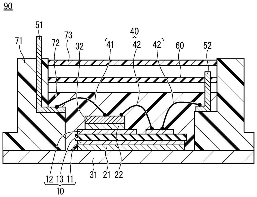
[0018] figure 1 It is a cross-sectional view showing an example of the structure of the semiconductor device 90 according to the first embodiment. The semiconductor device 90 has an insulating substrate 10 (first substrate), a soldering portion 21, a soldering portion 22, a base plate 31, at least one semiconductor chip 32 (semiconductor component), a plurality of wires 40, a plurality of main electrodes 51, and drive electrodes. 52. Printed wiring board 60 (second substrate), case 71, sealing material 72, and cover 73. The insulating substrate 10 includes: an insulating plate 13 having a first surface and a second surface (a lower surface and an upper surface in the figure); a conductor layer 11 provided on the first surface; and a conductor layer 12 provided on the second surface. 2 sides, with pattern. The plurality of wires 40 includes a main wire 41 and a driving wire 42 .

[0019] The housing 71 has a space closed by combining the base plate 31 and the cover 73 , and ...

Embodiment approach 2

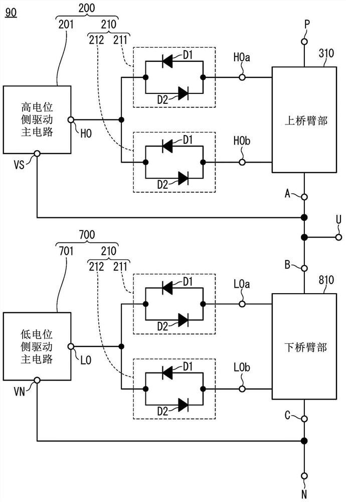
[0035] refer to Figure 5 , the semiconductor device according to Embodiment 2 has a plurality of insertion circuits 220 instead of a plurality of insertion circuits 210 ( image 3 : Embodiment 1). Each of the plurality of insertion circuits 220, in other words, each of the first insertion circuit 221 and the second insertion circuit 222 includes a first resistance element R1 connected in series with the first diode D1 and in parallel with the second diode D2, and a first resistance element R1 connected in series with the second diode D2 and in parallel with the second diode D2. The first diode D1 is connected in parallel to the second resistance element R2. In addition, since the structure other than this is substantially the same as the structure of Embodiment 1 mentioned above, the same code|symbol is attached|subjected to the same or corresponding element, and the description is not repeated.

[0036] According to this embodiment, when the current caused by the parasitic...

Embodiment approach 3

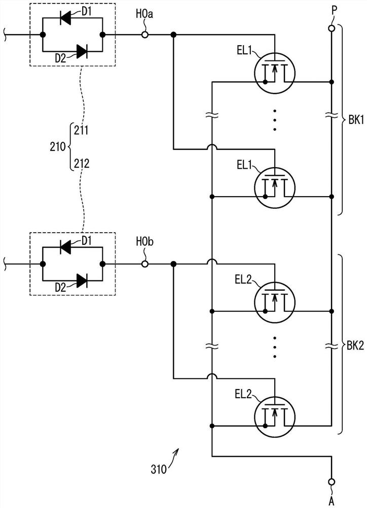
[0039] refer to Image 6 , the semiconductor device according to Embodiment 3 has an upper arm portion 320 instead of the upper arm portion 310 ( Figure 5 : Embodiment 2). In the upper arm portion 320 , a gate resistance element RG is provided between the insertion circuit 220 of the driving circuit and each of the plurality of semiconductor elements EL. Furthermore, although illustration is omitted, a gate resistance element RG is similarly provided in the lower arm portion. The gate resistance element RG may be a resistance element built into the semiconductor chip 32 on which the semiconductor element EL is formed, or may be a resistance element added separately from the semiconductor chip.

[0040] According to the present embodiment, the plurality of first semiconductor elements EL1 and the plurality of second semiconductor elements EL2 are separated by the gate resistance element RG. Therefore, even if the number of the plurality of first semiconductor elements EL1 a...


PUM


Abstract

Provided is a semiconductor device in which parasitic oscillation between a plurality of semiconductor elements connected in parallel with each other can be suppressed by a simple configuration. The plurality of semiconductor elements (EL) connected in parallel include a plurality of first semiconductor elements (EL1) and a plurality of second semiconductor elements (EL2). A drive circuit (200) for supplying a gate signal to each of a plurality of semiconductor elements (EL) includes a main circuit (201) and a plurality of insertion circuits (210) including a first insertion circuit (211) and a second insertion circuit (212). The first insertion circuit (211) is inserted between the main circuit (201) and the plurality of first semiconductor elements (EL1). A second insertion circuit (212) is inserted between the main circuit (201) and the plurality of second semiconductor elements (EL2). Each of the first insertion circuit (211) and the second insertion circuit (212) includes a first diode (D1) forward facing the main circuit (201) and a second diode (D2) reversely connected in parallel with the first diode (D1).

Description

technical field [0001] The present invention relates to a semiconductor device, and in particular, to a semiconductor device having a plurality of semiconductor elements connected in parallel to each other. Background technique [0002] A power semiconductor device often has a semiconductor element as a switching element. For example, a semiconductor element having a gate electrode such as MOSFET (Metal Oxide Semiconductor Field Effect Transistor) or IGBT (Insulated Gate Bipolar Transistor) is used. In particular, semiconductor devices for high power often have switching elements connected in parallel to each other. In a semiconductor device, a positive feedback circuit may be formed by parasitic capacitance and stray inductance of semiconductor elements. As a result, parasitic oscillation occurs, and the parasitic oscillation tends to become severe in proportion to the number of parallel-connected semiconductor elements. Therefore, a circuit for suppressing this parasitic...

Claims


Application Information

Patent Timeline
Patent Type & Authority Applications(China)
IPC IPC(8): H02M1/088H03K17/16H03K17/687
CPCH02M1/088H03K17/161H03K17/687H01L2224/73265H01L2224/48091H01L2924/181H01L2224/48227H01L2924/19107H01L2224/48464H01L23/053H01L2224/48157H01L2924/10272H02M7/5387H01L2224/32238H01L2224/32225H01L2224/291H01L2924/00014H01L2924/00012H01L2924/00H01L2924/014H01L25/165H01L29/1608H01L23/49822H01L24/48
Inventor 益田明宜宫崎裕二
Owner MITSUBISHI ELECTRIC CORP
Why Eureka
Try Eureka