
A Chip Clamping and Fixing and Chip Parallelism Measuring Structure for Ultrasonic Bonding

A clamping and fixing, ultrasonic bonding technology, applied in the direction of measuring devices, mechanical measuring devices, workpiece clamping devices, etc., can solve the problems of worn chip back, difficult relative displacement, reduced bonding efficiency, etc., to reduce mutual Friction, the effect of improving the utilization rate

Active Publication Date: 2021-11-16
SOUTHEAST UNIV
View PDF0 Cites 0 Cited by
  • Summary
  • Abstract
  • Description
  • Claims
  • Application Information

AI Technical Summary

Problems solved by technology

If the flip chip is not parallel to the substrate during the bonding process, it will greatly affect the bonding quality and the coupling between the chip and the substrate; If the back connection is unstable, the relative displacement between the suction nozzle and the back of the chip will occur during the bonding process, which will wear the back of the chip and affect the final performance of the device. It may also cause the chip to be damaged or even worn out, resulting in the prepared device becoming a waste product , reducing the bonding efficiency
[0005] In order to prevent the occurrence of non-parallel between the chip and the substrate or the relative displacement between the nozzle and the chip during the ultrasonic bonding process, it is necessary for the nozzle to have high requirements on the fixing ability of the chip, and at the same time, there must be a certain degree of parallelism between the chip and the substrate. High requirements, the relative displacement between the nozzle and the chip can be prevented to a certain extent by using a large negative pressure nozzle, but it is difficult to control the relative displacement within a certain degree when facing different ultrasonic energy inputs. At the same time, the measurement of the parallelism between the chip and the substrate needs to be accurate and simple, so as to achieve accurate and fast parallelism adjustment during the bonding process

Method used


Image

  • A Chip Clamping and Fixing and Chip Parallelism Measuring Structure for Ultrasonic Bonding
  • A Chip Clamping and Fixing and Chip Parallelism Measuring Structure for Ultrasonic Bonding
  • A Chip Clamping and Fixing and Chip Parallelism Measuring Structure for Ultrasonic Bonding

Examples


Embodiment Construction

[0028] The technical solutions of the present invention will be described in detail below in conjunction with the accompanying drawings.

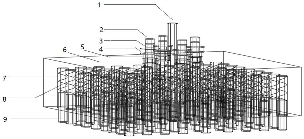
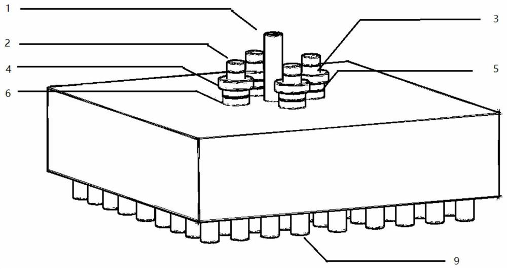
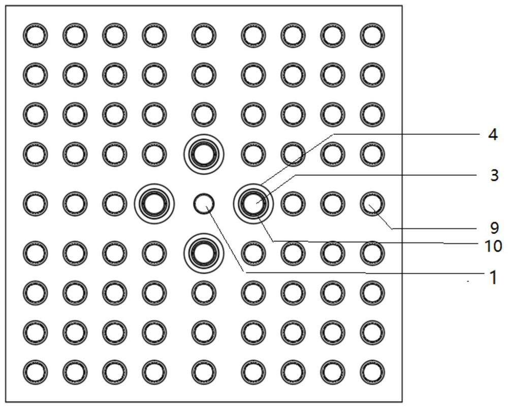
[0029] The invention designs a structure for ultrasonic flip-chip bonding chip clamping and chip parallelism measurement, which includes a long-pin chip parallelism measurement structure near the suction nozzle and a short-pin chip clamping and fixing structure outside.

[0030] like Figure 1-3 As shown, the long stitch parallelism measuring structure includes four fixing holes 10 , and the fixing holes 10 are evenly distributed around the suction nozzle 1 in a 90° distribution. 4 identical long pins 3 are located in the fixing holes 10 and can move up and down. The diameter of the long pins 3 is slightly smaller than the diameter of the fixing holes. Near the upper end of the long pin 3, an anti-falling cylindrical ring 4 with a diameter larger than the fixing hole 10 is arranged to prevent the long pin 3 from falling, and at the same ti...


PUM


Abstract

The invention discloses a chip clamping and fixing and chip parallelism measuring structure for ultrasonic bonding, comprising a long-pin chip parallelism measuring structure close to a suction nozzle and a short-pin chip clamp outside the long-pin chip parallelism measuring structure maintain a fixed structure. According to the principle of the sliding rheostat, the invention can accurately read the offset of chip parallelism by measuring the resistance change caused by the position change of the long pins, and through the determination formula of resistance, so as to realize accurate chip parallelism measurement and solve the problem of When the suction nozzle is parallel to the substrate, there may be external factors such as non-parallel chips caused by the height of the electrical contact bumps. In addition, during the ultrasonic bonding process of the short pins, the unfolded part can fix the position of the chip, thereby protecting the chip and increasing the bonding efficiency.

Description

technical field [0001] The invention belongs to the technical field of chip bonding and packaging, and in particular relates to a chip clamping and fixing and chip parallelism measuring structure. Background technique [0002] Chip interconnection technology affects the volume, performance and cost of microelectronic products. The commonly used chip interconnection technologies include wire bonding, automatic tape welding and flip chip bonding. Among these technologies, the wire bonding technology has the highest market share. Although the wire bonding process is simple and low in cost, there are some disadvantages, especially with the development of miniaturization and light weight of RF module products, chips The number of pins increases, and the I / O leads using wire bonding technology are arranged around the chip, and wire bonding will lead to an increasing volume. However, with flip-chip technology, the I / O leads can be arranged on the surface of the chip in an array, s...

Claims


Application Information

Patent Timeline
Patent Type & Authority Patents(China)
IPC IPC(8): B25B11/00G01B7/30G01B5/00
CPCB25B11/00G01B5/0002G01B7/30
Inventor 刘旭李昱宏王中武施晓亭孙小菡
Owner SOUTHEAST UNIV
Learn More