Method for judging the conductivity type of a semiconductor material in non-contact manner

A non-contact, conductive type of technology, applied in the direction of semiconductor characterization, single semiconductor device testing, electrical measurement, etc., can solve the problems of complex process, slow speed, wrong conclusion, etc., and achieve the effect of simple operation process

Active Publication Date: 2020-11-10
HANGZHOU DIANZI UNIV
View PDF9 Cites 0 Cited by
  • Summary
  • Abstract
  • Description
  • Claims
  • Application Information

AI Technical Summary

Problems solved by technology

This method has the following disadvantages: 1) This method is only applicable to SiC materials; 2) For wafers that are polished on the front but sandblasted on the back, it is difficult to measure the transmission spectrum (the absorption spectrum is generally obtained by converting the transmission spectrum, and the wafers that are sandblasted on the back cannot transmit light), so it is difficult to obtain the data of the forbidden band width; 3) the method of determining the forbidden band width from the transmission spectrum is not standardized enough, which can easily cause errors in the measurement of the forbidden band width, so as to draw wrong conclusions. Strictly speaking, it should be in accordance with Tauc The tangent method defined by the equation determines the bandgap width; 4) Due to the complexity of the process from measuring the absorption spectrum and calculating the bandgap width, manual participation is required, and the speed is slow, so it is difficult to realize automated mass screening

Method used


Image

  • Method for judging the conductivity type of a semiconductor material in non-contact manner

Examples


Embodiment Construction

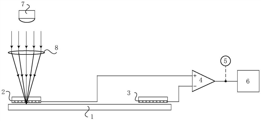
[0015] Such as figure 1 As shown, a non-contact method for judging the conductivity type of semiconductor materials, specifically:

[0016] A measurement electrode 2 and a reference electrode 3 are arranged above the surface of the semiconductor wafer 1 to be measured. The measuring electrode 2 and the reference electrode 3 are transparent conductive glass with the same size and shape. The orthographic projections of the measuring electrode 2 and the reference electrode 3 are within the scope of the semiconductor wafer 1 to be tested, and the mutual center distance between the two is greater than 3 times of the size of the electrodes themselves.

[0017] The measuring electrode 2 and the reference electrode 3 are close to the surface of the semiconductor wafer 1 to be measured, and its conductive surface faces downward, facing the surface of the semiconductor wafer 1 to be measured, and the distance between the measuring electrode 2 and the reference electrode 3 is the same a...


PUM


Abstract

The invention discloses a method for judging the conductivity type of a semiconductor material in a non-contact manner. According to an existing method, the surface of a semiconductor material is damaged after testing. According to the method, a measuring electrode and a reference electrode are arranged above the surface of a semiconductor wafer to be measured, the electrodes are transparent conductive glass, and the conductive surface is downward; the conductive surfaces of the two electrodes are respectively connected with the non-inverting input end and the inverting input end of the operational amplifier; and a heating light source is arranged above the measuring electrode. The light source is turned off, the output voltage of the operational amplifier is adjusted to 0, the light source is turned on to heat the local surface of the wafer, and the light source is turned off when the operational amplifier outputs a signal; 3-5 seconds later, the output voltage polarity of the operational amplifier is detected, and if the polarity is positive, the semiconductor material is of a P type; and if the polarity is negative, the semiconductor material is N-type. According to the method,sample damage is avoided, operation is easy, automation is easy to achieve, and meanwhile it is avoided that due to heating, the semiconductor material enters an intrinsic excitation state, judgment fails or misjudgment is caused.

Description

technical field [0001] The invention belongs to the technical field of semiconductors and relates to a non-contact method for judging the conductivity type of semiconductor materials. Background technique [0002] The conductivity type of semiconductor materials is one of the important parameters of semiconductor materials. The donor-doped semiconductor material is N-type, and the conduction is dominated by conduction band electrons; the acceptor-doped semiconductor material is P-type, and the conduction is dominated by valence band holes. In research and production, technicians often need to know the conductivity type of semiconductor materials. Commonly used methods to judge the conductivity type of semiconductor materials include thermoelectric potential, rectification, Hall effect, etc. The thermoelectric potential method can be divided into hot probe method and cold probe method. The above-mentioned methods all have a common shortcoming, that is, probes or electrodes...

Claims


Application Information

Patent Timeline
Patent Type & Authority Applications(China)
IPC IPC(8): G01R31/26
CPCG01R31/2601G01R31/2648
Inventor 季振国李阳阳席俊华
Owner HANGZHOU DIANZI UNIV
Why Eureka
Try Eureka