Electrostatic protection structure, display panel with electrostatic protection function and display device
A static protection and display panel technology, applied in the direction of static indicators, circuits, electrical components, etc., can solve the problems of limited electrostatic protection ability, achieve the effect of improving electrostatic protection ability, flexible use, and preventing electrostatic damage
- Summary
- Abstract
- Description
- Claims
- Application Information
AI Technical Summary
Problems solved by technology
Method used
Image
Examples
Embodiment 1
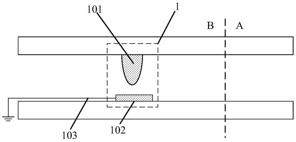
[0036] See figure 1 , figure 1 It is a structural schematic diagram of an electrostatic protection structure provided by an embodiment of the present invention. As shown in the figure, the static electricity protection structure 1 includes a static electricity collecting unit 101, a static electricity deriving unit 102 and a grounding wire 103, wherein the static electricity collecting unit 101 and the static electricity deriving unit 102 are arranged opposite to each other and at a certain distance from each other, and the static electricity deriving unit 102 and The ground wire 103 is connected, and the ground wire 103 is connected to the ground terminal.
[0037] Specifically, the static electricity collection unit 101 includes a discharge tip for collecting the charge on the color filter substrate 2 and transmitting it to the static electricity deriving unit 102 , and the static electricity deriving unit 102 is used for transmitting the static electricity to the ground te...
Embodiment 2
[0053] On the basis of the above embodiments, this embodiment further describes the specific structure of the electrostatic protection structure 1 .
[0054] Specifically, see Figure 7 , Figure 7 It is a detailed structural schematic diagram of an electrostatic protection structure provided by an embodiment of the present invention. In this embodiment, the electrostatic collection unit 101 is disposed on the lower surface of the color filter substrate 2 and includes a pad layer 111 and a conductive layer 112 covering the pad layer 111 . After the color filter substrate 2 and the thin-film transistor array substrate 3 are bonded, there is a certain distance between the color filter substrate 2 and the thin-film transistor array substrate 3, and the tip discharge generated by the static electricity collecting unit 101 and the static electricity deriving unit 102 needs to satisfy A certain distance condition, therefore, the electrostatic collection unit 101 includes a pad lay...
Embodiment 3
[0068] In this embodiment, on the basis of the above-mentioned embodiments, the display panel with an electrostatic protection function is mainly introduced.
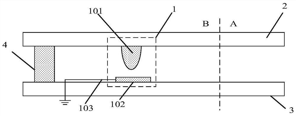
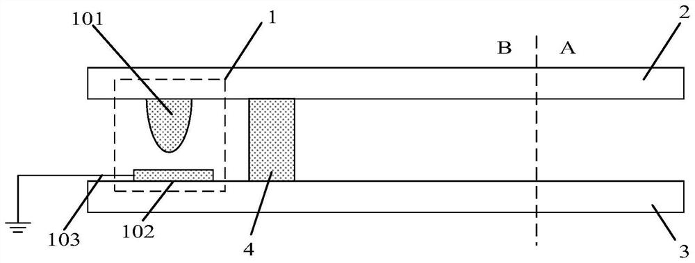
[0069] Specifically, the display panel includes a color filter substrate 2 and a thin film transistor array substrate 3 oppositely arranged, and a plurality of electrostatic protection structures described in the above-mentioned embodiments are arranged between the color filter substrate 2 and the thin film transistor array substrate 3 1. Wherein, the static electricity protection structure 1 has been introduced in detail in the foregoing embodiments, and will not be repeated here. The display panel may also include a display area A and a non-display area B located around the display area A, wherein the liquid crystal molecules are all distributed in the display area A, a plurality of the static electricity protection structures 1, that is, static electricity collecting units 101, static electricity Both the lead-out u...
PUM
| Property | Measurement | Unit |
|---|---|---|
| thickness | aaaaa | aaaaa |
Abstract
Description
Claims
Application Information


