Novel low-capacitance TVS structure and manufacturing method thereof
A manufacturing method and low-capacitance technology, applied in the manufacturing of circuits, electrical components, semiconductor/solid-state devices, etc., can solve the problems of high difficulty and high manufacturing cost, and achieve the effect of low manufacturing cost, low manufacturing cost, and low difficulty to achieve
- Summary
- Abstract
- Description
- Claims
- Application Information
AI Technical Summary
Problems solved by technology
Method used
Image


Examples
Embodiment Construction
[0029] In order to make the object, technical solution and advantages of the present invention clearer, the present invention will be further described in detail below in conjunction with the accompanying drawings and embodiments. It should be understood that the specific embodiments described here are only used to explain the present invention, not to limit the present invention.
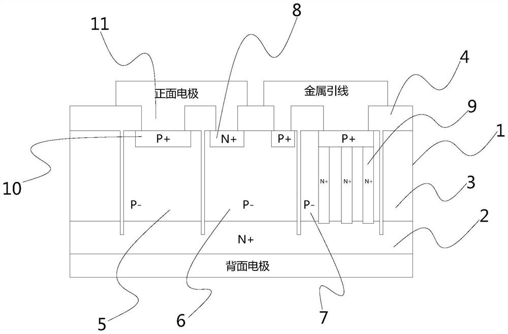
[0030] see Figure 1 to Figure 2 , a novel low-capacitance TVS structure disclosed by the invention, comprising a high-resistance substrate 1, on which a first doped layer 2 is formed by a triple diffusion process, and located above the first doped layer 2 The high-resistance layer 3 has a thickness less than 100 um, and this thickness can effectively improve the control capability of subsequent production lines to obtain a good high-resistance layer 3 .
[0031] The high-resistance layer 3 is provided with several trench isolation structures 4, and the bottom ends of the trench isolation structur...
PUM
 Abstract
Description
Claims
Application Information