
Analog-to-digital conversion device and method based on optical channelization

A technology of analog-to-digital conversion and analog-to-digital converter, which is applied in the field of microwave photonics, can solve problems such as difficult debugging, limited sampling bandwidth and ENOB of photonic analog-to-digital conversion devices, and limited delay matching accuracy, so as to enhance system reliability and stability performance, avoiding high spurious problems, and reducing hardware complexity

Active Publication Date: 2020-11-20
AEROSPACE INFORMATION RES INST CAS
View PDF3 Cites 0 Cited by
  • Summary
  • Abstract
  • Description
  • Claims
  • Application Information

AI Technical Summary

Problems solved by technology

However, due to the use of a similar architecture, there are the same problems as the traditional time-alternating analog-to-digital conversion device, namely: (1) this scheme requires that the time interval between any adjacent pulse trains be strictly consistent, while the actual time interval between optical pulse trains The delay matching accuracy is limited, and it will introduce always correlated spurs in the output of the photonic analog-to-digital conversion device; (2) the scheme also requires the subsequent processing links corresponding to each optical sampling pulse train (including filtering, amplification, photoelectric conversion and The transfer characteristics of quantization and other processes) are strictly consistent, which is also difficult to achieve in practice, thus introducing sampling clock-related nonlinear distortion in the final output
In addition, the key component of this type of photonic analog-to-digital conversion device-the high repetition rate ultra-narrow optical pulse source has problems such as complex structure, difficult debugging and low system stability.
These problems further increase the system complexity and application difficulty, weaken the reliability of the system, limit the sampling bandwidth and ENOB of the photonic analog-to-digital conversion device, and its practical application

Method used


Image

  • Analog-to-digital conversion device and method based on optical channelization
  • Analog-to-digital conversion device and method based on optical channelization
  • Analog-to-digital conversion device and method based on optical channelization

Examples


Embodiment Construction

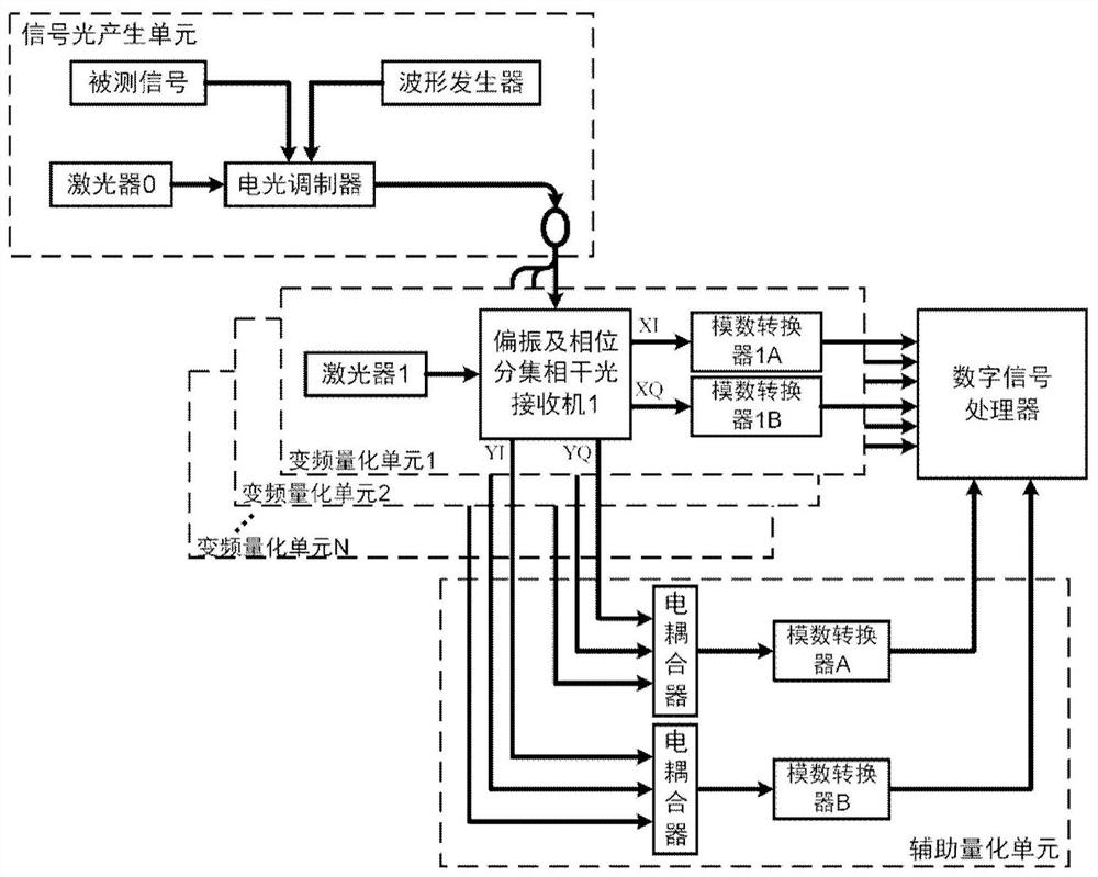
[0039]The invention discloses an analog-to-digital conversion method and device based on optical channelization. By using heterodyne optical channelization technology, the measured signal is divided into several channels in the frequency domain, and each channel is quantized separately, which effectively reduces the sampling frequency required for analog-to-digital conversion of large bandwidth signals, and breaks through the sampling bandwidth and sampling accuracy trade-off relationship. In addition, the present invention also has the advantages of simple structure and strong tunability, and can meet various application requirements.

[0040] Specifically, the present invention discloses an analog-to-digital conversion device based on optical channelization, such as figure 1 As shown, it includes a signal light generation unit, N parallel frequency conversion and quantization units, auxiliary quantization units and digital signal processing units; wherein the signal light g...


PUM


Abstract

An analog-to-digital conversion device based on optical channelization comprises a signal light generation unit, N parallel frequency conversion quantization units, an auxiliary quantization unit anda digital signal processing unit, wherein the signal light generation unit is connected with the N parallel frequency conversion quantization units through polarization maintaining optical fibers; theN parallel frequency conversion quantization units are connected with the auxiliary quantization unit through coaxial radio frequency cables; and the N parallel frequency conversion quantization units and the auxiliary quantization unit are connected with the digital signal processing unit through a communication protocol. According to the invention, a measured signal is cut into a plurality of narrow bands in a frequency domain by using an optical channelization technology, and the narrow bands are quantized respectively, so that the sampling frequency is greatly reduced, and the problem ofhigh stray caused by jittering of the sampling aperture under the high sampling frequency is avoided; and under the same sampling bandwidth, the significant digit of the method is obviously improved compared with that of a disclosed analog-to-digital conversion method.

Description

technical field [0001] The present invention relates to the field of microwave photon technology, in particular to an analog-to-digital conversion device and method based on optical channelization. Background technique [0002] An analog-to-digital converter (Analog to digital converter, ADC) is a type of device that converts analog electrical signals into digital signals. Today, as the complexity of signal processing algorithms continues to increase, signal processing methods based on digital technology have become mainstream. As a key device connecting the analog domain and the digital domain, the ADC has become an essential part of most electronic systems. With the continuous expansion and deepening of the application field of electronic technology, the conversion bandwidth and precision of analog-to-digital converters have been rapidly improved. However, the existing analog-to-digital converter architecture based on traditional electronic technology and devices has pro...

Claims


Application Information

Patent Timeline
IPC IPC(8): G02F7/00
CPCG02F7/00
Inventor 李王哲杨继尧刘宸钰董婧雯
Owner AEROSPACE INFORMATION RES INST CAS
Learn More