Semiconductor process equipment and processing method of focusing ring

A process equipment and semiconductor technology, applied in semiconductor/solid-state device manufacturing, discharge tubes, electrical components, etc., can solve the problem of inability to eliminate the etching tilt effect at the edge of the wafer, so as to offset the etching tilt effect and improve the process effect. Effect

Pending Publication Date: 2020-11-20
BEIJING NAURA MICROELECTRONICS EQUIP CO LTD
View PDF0 Cites 1 Cited by
  • Summary
  • Abstract
  • Description
  • Claims
  • Application Information

AI Technical Summary

Problems solved by technology

[0005] The purpose of the embodiment of the present application is to provide a semiconductor process equipment and a processing method of the focus ring to solve the problem that the prior art cannot eliminate the etching tilt effect at the edge of the wafer

Method used


Image

  • Semiconductor process equipment and processing method of focusing ring
  • Semiconductor process equipment and processing method of focusing ring
  • Semiconductor process equipment and processing method of focusing ring

Examples


Embodiment Construction

[0036] The embodiment of the present application provides a semiconductor process equipment and a processing method of a focus ring, which are used to solve the problem that the etching tilt effect at the edge of the wafer cannot be eliminated in the prior art.

[0037] In order to enable those skilled in the art to better understand the technical solutions in the present application, the technical solutions in the embodiments of the present application will be clearly and completely described below in conjunction with the drawings in the embodiments of the present application. Obviously, the described The embodiments are only some of the embodiments of the present application, but not all of them. Based on the embodiments in this application, all other embodiments obtained by persons of ordinary skill in the art without creative efforts shall fall within the scope of protection of this application.

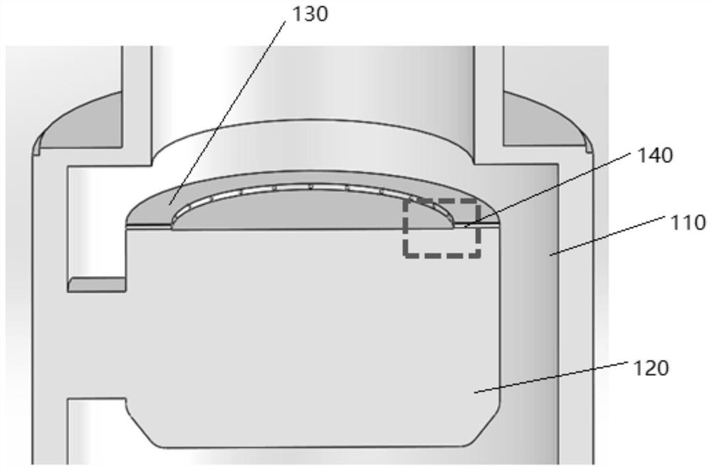
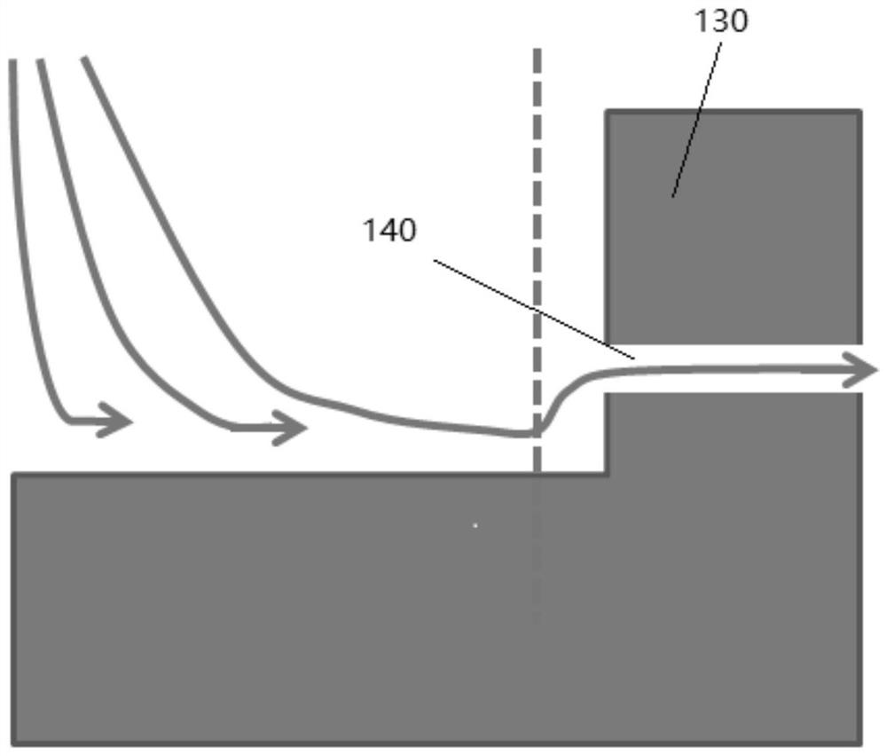
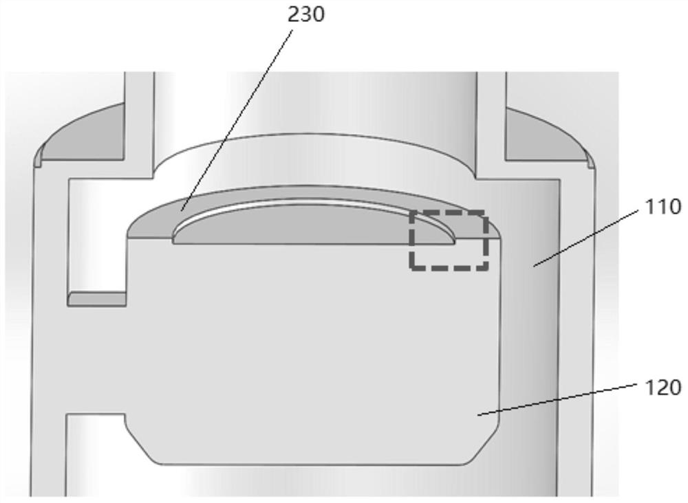
[0038] Fig. 1 (a) is a schematic cross-sectional view of a semiconductor pro...


PUM


Abstract

The embodiment of the invention discloses semiconductor process equipment and a processing method of a focusing ring and aims to solve the problem that the etching inclination effect of the edge of awafer cannot be eliminated in the prior art. The semiconductor process equipment comprises a process chamber and a base located in the process chamber; the base is used for bearing a wafer; a focusingring is arranged on the base; and when the base bears the wafer, the focusing ring surrounds the outer side of the wafer; the focusing ring is provided with an air flow channel, and the air flow channel is used for guiding process gas on the surface of the wafer to the outer side of the base so as to adjust the air flow field of the edge part of the wafer and counteract the etching inclination effect of an electromagnetic field on the edge part. The equipment can effectively eliminate the etching inclination effect of the edge area in the wafer processing process.

Description

technical field [0001] The invention relates to the technical field of semiconductors, in particular to a semiconductor process equipment and a processing method for a focus ring. Background technique [0002] Deep silicon etching is a very important process for manufacturing microstructures in industrial production, and can be applied to fields such as microelectromechanical systems, microfluidic devices, and advanced packaging. In actual production, improving the etching processability in the etching chamber and wafer (the current mainstream production line has a wafer size of 6 inches, 8 inches and 12 inches, etc.) can reduce production costs. As the size of the wafer increases, it poses a greater challenge to the etching uniformity of the etching machine. Among them, the uniformity can be subdivided into the uniformity of the etching profile and the uniformity of the etching depth. Due to the influence of the edge effect, the electromagnetic field will be distorted at ...

Claims


Application Information

Patent Timeline
Patent Type & Authority Applications(China)
IPC IPC(8): H01J37/21H01J37/305H01J37/32H01L21/3065
CPCH01J37/21H01J37/3053H01J37/3056H01J37/32385H01J37/32642H01J37/32834H01L21/3065
Inventor 唐希文林源为王春
Owner BEIJING NAURA MICROELECTRONICS EQUIP CO LTD
Why Eureka
Try Eureka