Substrate for PERC battery, and PERC battery and preparation method thereof
A substrate and battery technology, applied in the field of solar cells, can solve problems such as low battery efficiency, high contact resistance, and inability to fill edge areas
- Summary
- Abstract
- Description
- Claims
- Application Information
AI Technical Summary
Problems solved by technology
Method used
Image
Examples
Embodiment 1
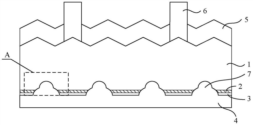
[0070] This embodiment provides a PERC battery, such as figure 1 , Figure 4 and Figure 5 As shown, it includes: a silicon wafer layer 1 with a PN junction, a back passivation layer 2, a protective layer 3 and a back field layer 4 arranged sequentially from the back of the silicon wafer layer 1 with a PN junction, and a back field layer 4 from the silicon wafer layer 1 with a PN junction. A front passivation layer 5 and a front electrode 6 arranged sequentially from the front side of the silicon wafer layer 1 outward;
[0071] The back passivation layer 2 and the protective layer 3 are provided with a plurality of periodically arranged grooves 7, the grooves 7 penetrate the back passivation layer 2 and the protective layer 3, and the part of the back field layer 4 located in the groove 7 is connected with the The silicon wafer layer 1 of the PN junction is connected;
[0072] The groove 7 includes a first groove area 71 and a second groove area 72 along the depth directio...
Embodiment 2
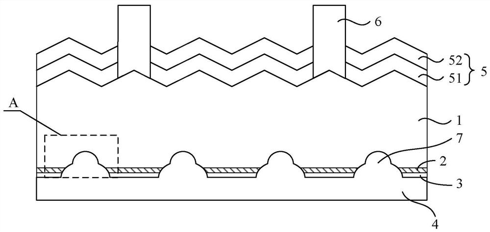
[0086]This embodiment provides a PERC battery, such as figure 2 , Figure 4 and Figure 5 As shown, it includes: a silicon wafer layer 1 with a PN junction, a back passivation layer 2, a protective layer 3 and a back field layer 4 arranged sequentially from the back of the silicon wafer layer 1 with a PN junction, and a back field layer 4 from the silicon wafer layer 1 with a PN junction. A front passivation layer 5 (consisting of a front first passivation layer 51 and a front second passivation layer 52) and a front electrode 6 are arranged sequentially from the front side of the silicon wafer layer 1 outward;
[0087] The back passivation layer 2 and the protective layer 3 are provided with a plurality of periodically arranged grooves 7, the grooves 7 penetrate the back passivation layer 2 and the protective layer 3, and the part of the back field layer 4 located in the groove 7 is connected with the The silicon wafer layer 1 of the PN junction is connected;
[0088] The...
Embodiment 3
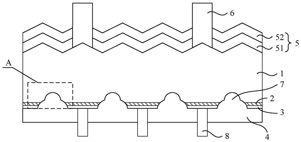
[0102] This embodiment provides a PERC battery, such as image 3 , Figure 4 and Figure 5 As shown, it includes: a silicon wafer layer 1 with a PN junction, a back passivation layer 2, a protective layer 3, a back field layer 4 and a back electrode 8 arranged sequentially from the back of the silicon wafer layer 1 with a PN junction outward, and from A front passivation layer 5 (consisting of a front first passivation layer 51 and a front second passivation layer 52) and a front electrode 6 are sequentially arranged on the front side of the silicon wafer layer 1 having a PN junction;
[0103] The back passivation layer 2 and the protective layer 3 are provided with a plurality of periodically arranged grooves 7, the grooves 7 penetrate the back passivation layer 2 and the protective layer 3, and the part of the back field layer 4 located in the groove 7 is connected with the The silicon wafer layer 1 of the PN junction is connected;
[0104] The groove 7 includes a first g...
PUM
| Property | Measurement | Unit |
|---|---|---|
| Depth | aaaaa | aaaaa |
| Depth | aaaaa | aaaaa |
| Opening diameter | aaaaa | aaaaa |
Abstract
Description
Claims
Application Information
 - R&D Engineer
- R&D Manager
- IP Professional
- Industry Leading Data Capabilities
- Powerful AI technology
- Patent DNA Extraction
Browse by: Latest US Patents, China's latest patents, Technical Efficacy Thesaurus, Application Domain, Technology Topic, Popular Technical Reports.
© 2024 PatSnap. All rights reserved.Legal|Privacy policy|Modern Slavery Act Transparency Statement|Sitemap|About US| Contact US: help@patsnap.com


