Image sensor pixel structure

An image sensor and pixel structure technology, applied in image communication, TV, color TV components, etc., can solve the problems of small dynamic range, unable to meet the needs of high dynamic range applications, etc., to improve dynamic range and high sensitivity. , the effect of increasing the full well capacity

Active Publication Date: 2020-11-27
BRIGATES MICROELECTRONICS KUNSHAN
View PDF5 Cites 1 Cited by
  • Summary
  • Abstract
  • Description
  • Claims
  • Application Information

AI Technical Summary

Problems solved by technology

[0005] However, although the existing CMOS image sensor has high photosensitive sensitivity, its dynamic range is small, which cannot meet the needs of high dynamic range applications under global exposure.

Method used


Image

  • Image sensor pixel structure
  • Image sensor pixel structure
  • Image sensor pixel structure

Examples


Embodiment Construction

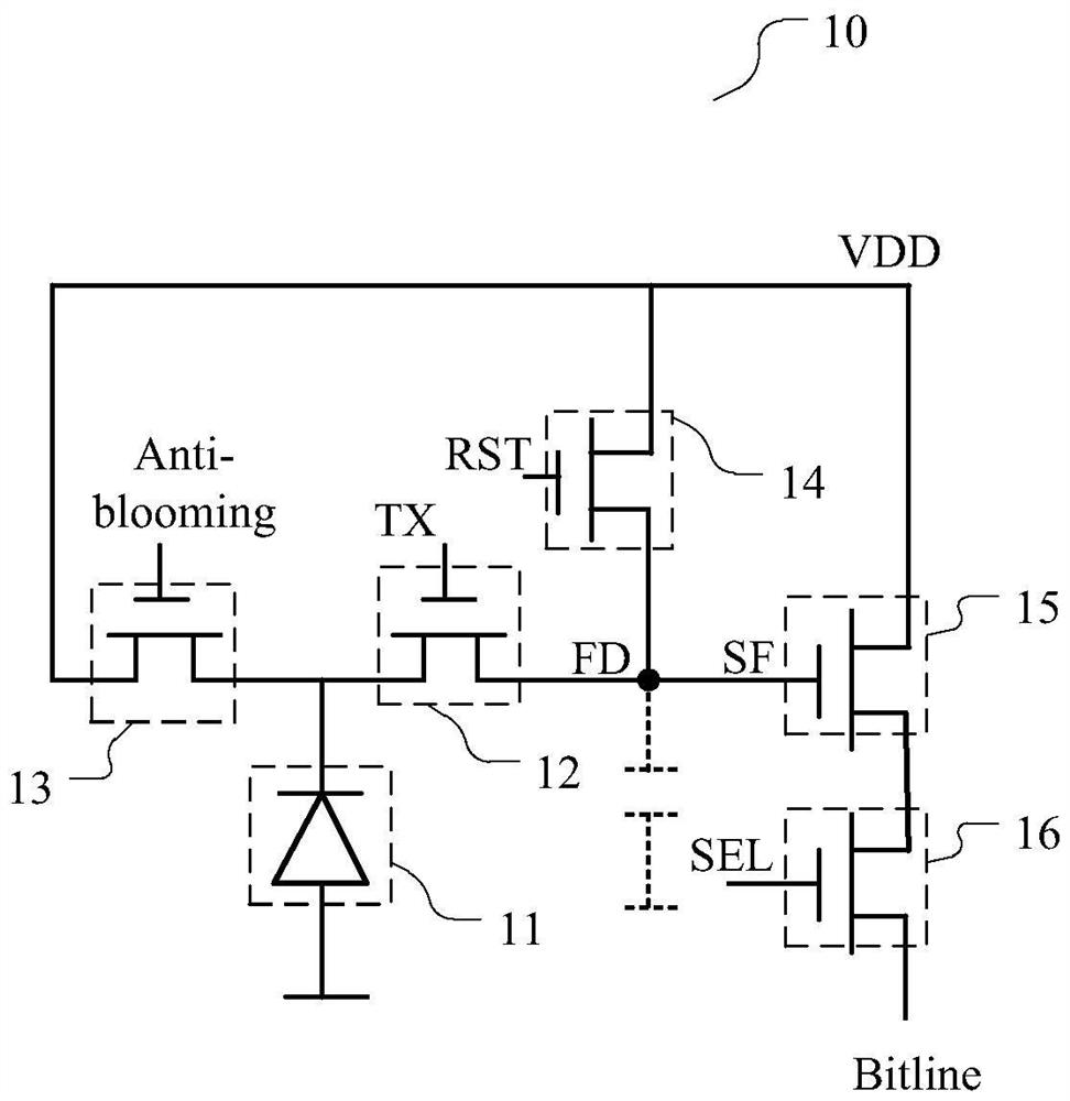
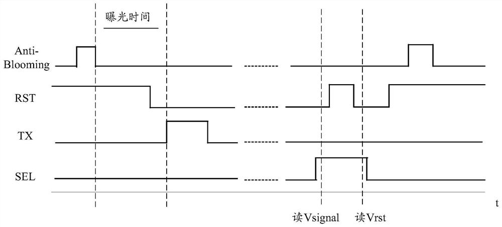
[0046] Dynamic range is a very important index parameter of image sensor. The dynamic range indicates the range of the maximum light intensity and the minimum light intensity that the image sensor can simultaneously detect in the same image, generally expressed in dB. The specific formula is as follows:

[0047]

[0048] Among them, P max Indicates the maximum detectable light intensity, P max Indicates the minimum detectable light intensity. The dynamic range of a general image sensor is between 60-70dB, and the dynamic range of the human eye is between 100-120dB. A high dynamic range image sensor is very important for maintaining the balance of details in the dark and details in the bright.

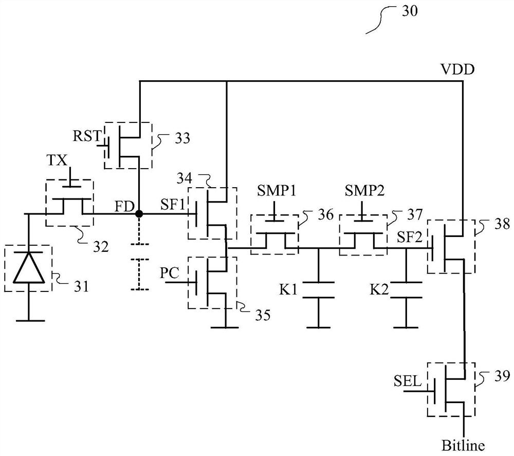
[0049] The full well capacity of an image sensor refers to the maximum number of electrons that can be collected and accommodated by the pixel structure. Large full well capacity can effectively improve the dynamic range of the image sensor. For general linear response image se...


PUM


Abstract

An image sensor pixel structure is suitable for obtaining a first frame of image and a second frame of image of a target scene in the same exposure process so as to fuse the first frame of image and the second frame of image into one frame of image. The pixel structure comprises a first charge storage circuit and a second charge storage circuit, the first charge storage circuit is coupled with thefloating diffusion node and is suitable for storing an exposure signal corresponding to the second frame image after exposure is finished; and the second charge storage circuit is coupled with the first source follower circuit and is suitable for storing an exposure signal and a reset signal corresponding to the first frame image after exposure is finished. By applying the scheme, the photosensitive sensitivity of the CMOS image sensor can be improved, and meanwhile, the CMOS image sensor has a relatively high dynamic range.

Description

technical field [0001] The invention relates to the field of semiconductor manufacturing, in particular to an image sensor pixel structure. Background technique [0002] An image sensor is a semiconductor device that converts light signals into electrical signals. [0003] Image sensors are classified into complementary metal oxide (Complementary Metal Oxide Semiconductor, CMOS) image sensors and charge coupled device (Charge Coupled Device, CCD) image sensors. Among them, the CMOS image sensor has the advantages of simple process, easy integration of other devices, small size, light weight, low power consumption and low cost. Therefore, with the development of image sensing technology, CMOS image sensors are increasingly used in various electronic products instead of CCD image sensors. [0004] In order to improve the dark light performance of the CMOS image sensor, it is necessary to increase the light sensitivity of the image sensor. [0005] However, although the exis...

Claims


Application Information

Patent Timeline
Patent Type & Authority Applications(China)
IPC IPC(8): H04N5/374
CPCH04N25/76
Inventor 王林黄金德
Owner BRIGATES MICROELECTRONICS KUNSHAN
Why Eureka
Try Eureka