Novel semiconductor silicon wafer circle-cutting equipment

A semiconductor and silicon wafer technology, applied in the field of new semiconductor silicon wafer cutting equipment, can solve the problems of circular silicon wafer scratches, easy edges, silicon wafer burrs, etc., and achieve the effect of reducing friction

Inactive Publication Date: 2020-12-04
菏泽景月装饰有限公司
View PDF0 Cites 1 Cited by
  • Summary
  • Abstract
  • Description
  • Claims
  • Application Information

AI Technical Summary

Problems solved by technology

[0004] In order to prevent too many scratches on the silicon wafer, a thin film is usually attached to the outer side of the silicon wafer. During the circle cutting work of the silicon wafer, the cutting is carried out together with the thin film. The edges are raised, resulting in film burrs on the edge of the silicon wafer after rounding, causing the film to be easily detached from the silicon wafer and causing scratches on the round silicon wafer

Method used


Image

  • Novel semiconductor silicon wafer circle-cutting equipment
  • Novel semiconductor silicon wafer circle-cutting equipment
  • Novel semiconductor silicon wafer circle-cutting equipment

Examples


Embodiment 1

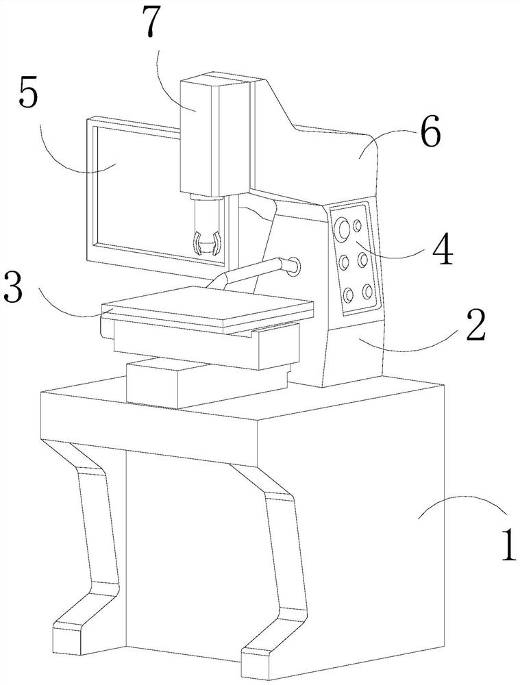
[0029] as attached figure 1 To attach Figure 6 Shown:

[0030] The invention provides a new type of semi-conductor silicon wafer cutting equipment, the structure of which includes a machine base 1, a control table 2, a working surface 3, a control panel 4, a system display screen 5, a rotating head 6, and a cutting head 7. The control table 2 Welded on the rear side of the top surface of the machine base 1, the worktable 3 is located in front of the control console 2, the control panel 4 and the control console 2 are integrated structures and are arranged on one side of the control console 2, the system The display screen 5 is fixedly connected to the other side of the control table 2 , the rotating head 6 is movably connected to the top of the control table 2 , and the cutting head 7 is connected to the front end of the rotating head 6 .

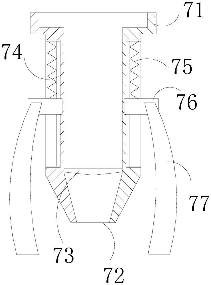
[0031] The cutting head 7 is provided with a columnar frame 71, a beam penetrating head 72, a focusing mirror 73, a guide rail 74, a sp...

Embodiment 2

[0037] as attached Figure 7 To attach Figure 8 Shown:

[0038] Wherein, the arc cavity 771 is provided with a movable chamber 71a, a first airbag 71b, a second airbag 71c, and an air intake drum 71d, and the movable chamber 71a is arranged between the first airbag 71b and the second airbag 71c, The intake drum 71d is at the upper end of the movable chamber 71a, the intake drum 71d is connected through the first air bag 71b and the second air bag 71c, and there is gas inside the first air bag 71b and the second air bag 71c. The air intake drum 71d is made of high-elastic rubber material, and the slow pressure wheel 772 slides inward along the inner side wall, squeezing the first air bag 71b and the second air bag 71c, so that the gas goes up, and the air intake drum 71d 71d is used as an elastic hollow ball to accommodate gas.

[0039] Wherein, the pulling cavity 773 is provided with a concave cavity 73a, an arc rail 73b, a push rod 73c, a roller 73d, and a rear pulling en...


PUM


Abstract

The invention discloses novel semiconductor silicon wafer circle-cutting equipment. The novel semiconductor silicon wafer circle-cutting equipment structurally comprises a machine base, a control console, a working table top, a control panel, a system display screen, a rotating head and a cutting head. A flattening block is subjected to arc bending due to obstruction of friction force, a slow pressing wheel makes contact with a silicon wafer to flatten burrs, when a soft pressing ring is stressed, the position of gas in an expansion block is changed, a sliding block pulls supporting steel to be diverged, the section, in contact with the silicon wafer, of the soft pressing ring is sunken and then rapidly recovers under the action of an elastic piece, it is guaranteed that when the soft pressing ring slides on the surface of the silicon wafer, no large hardness collision pressure is caused between the soft pressing ring and the silicon wafer, the slow pressing wheel sinks inwards under the counter-acting force to extrude gas at the lower ends of first and second airbags upwards, the gas enters a gas inlet drum ball so that the upper end of an arc cavity can be bulged to extrude a concave cavity, the concave cavity is bent in the arc direction to eject a movable ejector rod to pry a roller to slide upwards, a rear pulling end pulls the lower middle section of a pulling cavity, thepulling cavity is lifted to increase the distance from the surface of the silicon wafer, and therefore friction force is reduced.

Description

technical field [0001] The invention belongs to the field of semiconductors, and more specifically relates to a novel semiconductor silicon wafer cutting device. Background technique [0002] Silicon wafers are common and important semiconductor materials. Semiconductor silicon wafers with conductivity between conductors and insulators are sheet-shaped silicon wafers cut from silicon blocks. The circular cutting machine can pass high-energy laser beams on the surface of silicon wafers. Irradiated for further processing, cutting out circular silicon wafers. [0003] Based on the inventor's discovery above, there are following deficiencies in the existing novel semiconductor silicon wafer cutting equipment: [0004] In order to prevent too many scratches on the silicon wafer, a thin film is usually attached to the outer side of the silicon wafer. During the circle cutting work of the silicon wafer, the cutting is carried out together with the thin film. The edges will cause ...

Claims


Application Information

Patent Timeline
Patent Type & Authority Applications(China)
IPC IPC(8): B23K26/38B23K26/08B23K26/70B23K101/40
CPCB23K26/0853B23K26/38B23K26/702B23K2101/40
Inventor 傅梅英
Owner 菏泽景月装饰有限公司
Why Eureka
Try Eureka