SMT welding process for PCB in shell body

A technology of PCB board and welding process, which is applied in the field of SMT welding process of PCB board in the shell, which can solve the problems of prone to false soldering, low yield and low efficiency, etc., and achieve strong operability, high assembly efficiency and simple process Effect

Active Publication Date: 2020-12-04
YANGZHOU HAIKE ELECTRONICS TECH CO LTD
View PDF5 Cites 4 Cited by
  • Summary
  • Abstract
  • Description
  • Claims
  • Application Information

AI Technical Summary

Problems solved by technology

Since the PCB board has been installed in the shell, the traditional SMT process is no longer applicable, and related equipment such as automatic printing machines can no longer be used at this time, so it can only be completed by manual soldering and other methods.
However, for high-volume products, the efficiency is very low, and defects such as virtual soldering and bridges are prone to occur, and the yield rate is not high, especially for high-frequency boards of microwave components with high assembly density, this problem is particularly prominent, and grounding Pad solder can not wet and other defects

Method used


Image

  • SMT welding process for PCB in shell body
  • SMT welding process for PCB in shell body
  • SMT welding process for PCB in shell body

Examples


Embodiment

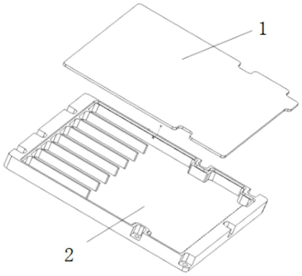
[0062] Such as figure 2 As shown, the housing used in this embodiment, the material of the housing cover plate 1 is 4A11 aluminum alloy, and the surface treatment method is natural color conductive oxidation. The material of shell cavity 2 is 6061 aluminum alloy, and the surface treatment method of shell cavity 2 is as follows: the soldering part of the PCB board is plated with nickel as a base, with a thickness of 5 μm, and then gold-plated on the surface, with a thickness of 0.5 μm, and the rest of the non-welding parts are used with natural color conductive oxidation . In order to ensure the tightness of the housing, the housing cover plate 1 is welded to the housing cavity 2 by means of laser sealing welding.

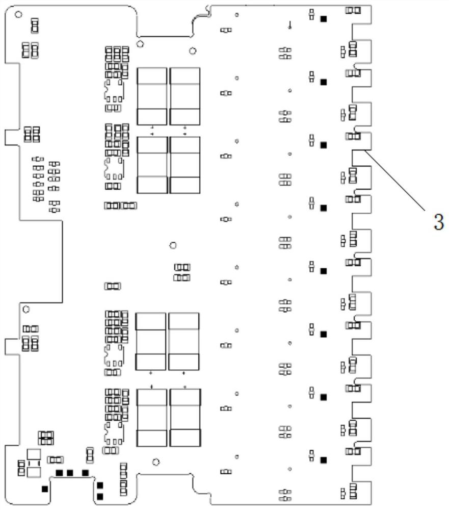
[0063] Such as image 3 As shown, the PCB board 3 used in the present invention is made of FR4+CLTE-XT and has a total thickness of 1.4 mm. Since the housing needs to be sealed, and the thickness of the housing cavity 2 is too small, the PCB board 3 cannot be in...


PUM


Abstract

The invention discloses an SMT welding process for a PCB in a shell body. The process comprises the following steps of: selecting materials of a shell body cover plate and a shell body cavity, and respectively carrying out surface treatment on the shell body cover plate and the shell body cavity; welding the PCB into the shell body cavity ; covering and fixing a frameless steel mesh on the PCB, wherein windows on the frameless steel mesh are in one-to-one correspondence with bonding pads on the PCB; printing solder paste on the bonding pads on the PCB through using the frameless steel mesh, and taking out the frameless steel mesh after printing is completed; using an automatic chip mounter to mount a surface-mount device on the PCB; and welding the surface-mounted device to a correspondingposition of the PCB through reflow soldering. According to the SMT welding process, manual printing and automatic chip mounting processes are adopted, the process is simple, the operability is high,the assembly efficiency is high, and SMT welding of large-batch and high-integration substrates can be met.

Description

technical field [0001] The invention relates to the technical field of electronic industry welding, in particular to an SMT welding process of a PCB board in a casing. Background technique [0002] SMT (Surface Mount Technology), also known as surface mount technology, is a board-level assembly technology that mounts surface mount components (SMD) on printed circuit boards (PCB), and is currently the most common in the electronic assembly industry. Technology and craftsmanship are also the core of modern electronic assembly technology. [0003] The SMT soldering process generally has two processes: reflow soldering and wave soldering. The reflow soldering process refers to melting the solder paste pre-printed on the PCB pad to realize the soldering end of the surface mount component or the mechanical connection between the introduction and the PCB pad. A soldering process for electrical connections. It includes the following steps: (1) Make a stencil, make a stencil with a...

Claims


Application Information

Patent Timeline
Patent Type & Authority Applications(China)
IPC IPC(8): H05K3/34H05K3/12
CPCH05K3/341H05K3/3452H05K3/1216H05K3/3494
Inventor 陈澄孙乎浩高修立
Owner YANGZHOU HAIKE ELECTRONICS TECH CO LTD
Why Eureka
Try Eureka