Communication link layer message single event effect fault tolerance method and device

A single event effect and communication link technology, which is applied in the field of a communication link layer message single event effect fault tolerance method and device, and achieves the effects of high reliability, prevention of false export, and high real-time performance.

Active Publication Date: 2020-12-08
NARI TECH CO LTD +1
View PDF3 Cites 1 Cited by
  • Summary
  • Abstract
  • Description
  • Claims
  • Application Information

AI Technical Summary

Problems solved by technology

[0010] Purpose of the invention: The purpose of the present invention is to provide a communication link layer message single event effect fault tolerance that is applicable to the secondary equipment of the power system and can cover the entire communication link to solve the system security problem caused by the wrong message output Method and device

Method used


Image

  • Communication link layer message single event effect fault tolerance method and device
  • Communication link layer message single event effect fault tolerance method and device
  • Communication link layer message single event effect fault tolerance method and device

Examples


Embodiment Construction

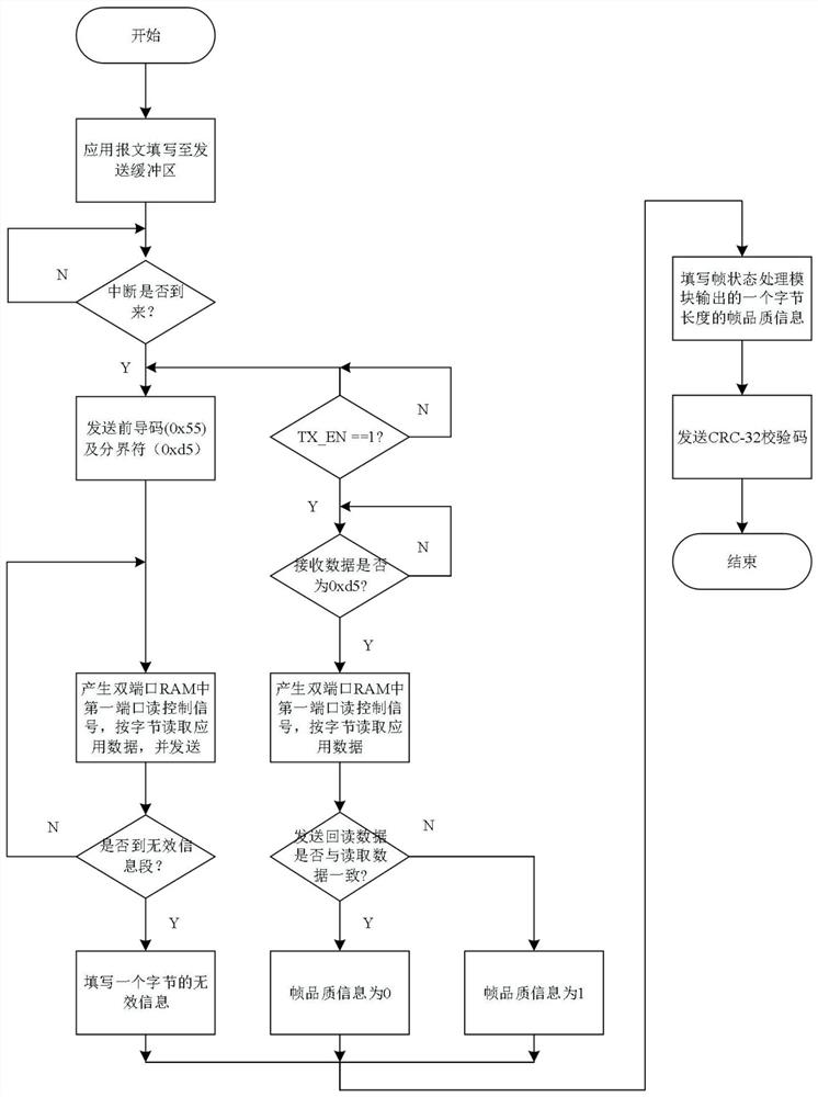
[0034] The present invention will be further described in detail below in conjunction with specific implementation methods and descriptions.

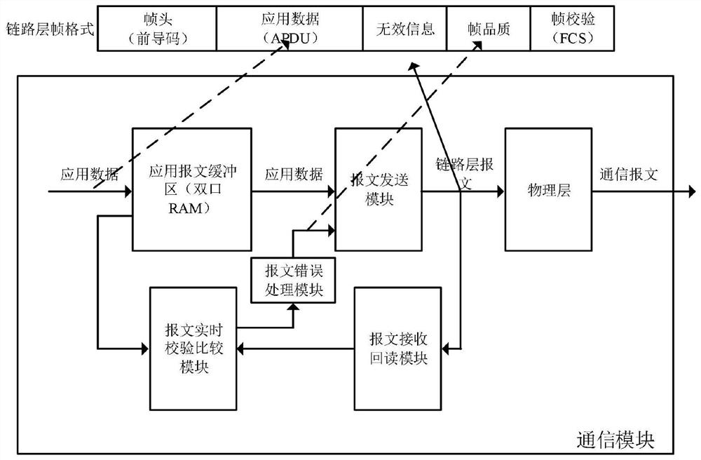
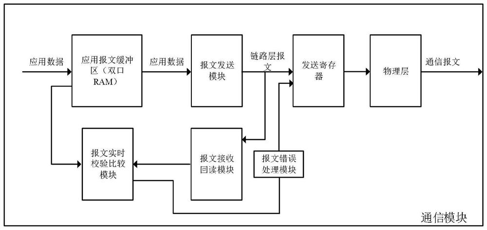
[0035] Such as figure 2 As shown, the communication link layer message single event effect fault-tolerant device of the present invention includes an application message buffer, a message sending module, a message receiving and reading back module, a message real-time verification and comparison module, and a message error processing module . The application message buffer is connected to the physical layer through the message sending module. The input end of the message receiving and reading back module is connected between the message sending module and the physical layer, and the output end of the message receiving and reading back module is connected with the message real-time verification and comparison module. A message error processing module is connected between the message real-time verification and comparison module and the...


PUM


Abstract

The invention discloses a communication link layer message single event effect fault tolerance method and device. The method comprises the steps of adding a message real-time read-back channel in an FPGA link layer, and comparing a real-time read-back message with original application data; and after data errors are judged,realizing fault-tolerant processing of the single event effect in the message transmission process of the communication link layer based on two error processing methods. The method provided by the invention does not depend on an external processor, can avoid the serious problems of protection maloperation and the like caused by SV and GOOSE message error output due to the influence of a single event effect on the FPGA, and greatly improves the reliability of the secondary equipment of a power system.

Description

technical field [0001] The invention relates to an integrated chip single event effect error detection and error correction method, in particular to a communication link layer message single event effect fault tolerance method and device. Background technique [0002] With the technological development of high-performance integrated circuits, it has become a mainstream trend to adopt high-performance integrated circuit chips such as general-purpose processors (CPUs) and programmable logic gate arrays (FPGAs) in power system secondary equipment. However, compared with traditional circuits, digital chips using integrated circuits have low operating voltage and complex design. A series of single event effects such as single event upset (SEU, Single Event Upset), single event function interruption and single event transient pulse will become more and more obvious. The anti-space radiation interference capability of integrated circuits in power system secondary equipment has gra...

Claims


Application Information

Patent Timeline
Patent Type & Authority Applications(China)
IPC IPC(8): G06F11/10G06F9/54
CPCG06F11/1004G06F9/544
Inventor 王海全姜雷周华良夏雨高诗航姚吉文邹志杨
Owner NARI TECH CO LTD
Why Eureka
Try Eureka