Insulated gate bipolar transistor and manufacturing method thereof

A technology for bipolar transistors and manufacturing methods, which is applied in semiconductor/solid-state device manufacturing, semiconductor devices, electrical components, etc., and can solve the problems that the performance of insulated gate bipolar transistors needs to be improved.

Pending Publication Date: 2020-12-08
SHANGHAI HUAHONG GRACE SEMICON MFG CORP
View PDF0 Cites 0 Cited by
  • Summary
  • Abstract
  • Description
  • Claims
  • Application Information

AI Technical Summary

Problems solved by technology

With the wide application of insulated gate bipolar transistors, in order to meet the requirements of high reverse withstand voltage and the reliability of reverse withstand voltage at higher temperatures (automotive grade requires 175 ° C), the insulated ga

Method used


Image

  • Insulated gate bipolar transistor and manufacturing method thereof
  • Insulated gate bipolar transistor and manufacturing method thereof
  • Insulated gate bipolar transistor and manufacturing method thereof

Examples


Embodiment Construction

[0034] The insulated gate bipolar transistor and its manufacturing method proposed by the present invention will be further described in detail below with reference to the accompanying drawings and specific embodiments. The advantages and features of the present invention will become clearer from the following description. It should be noted that all the drawings are in a very simplified form and use imprecise scales, and are only used to facilitate and clearly assist the purpose of illustrating the embodiments of the present invention.

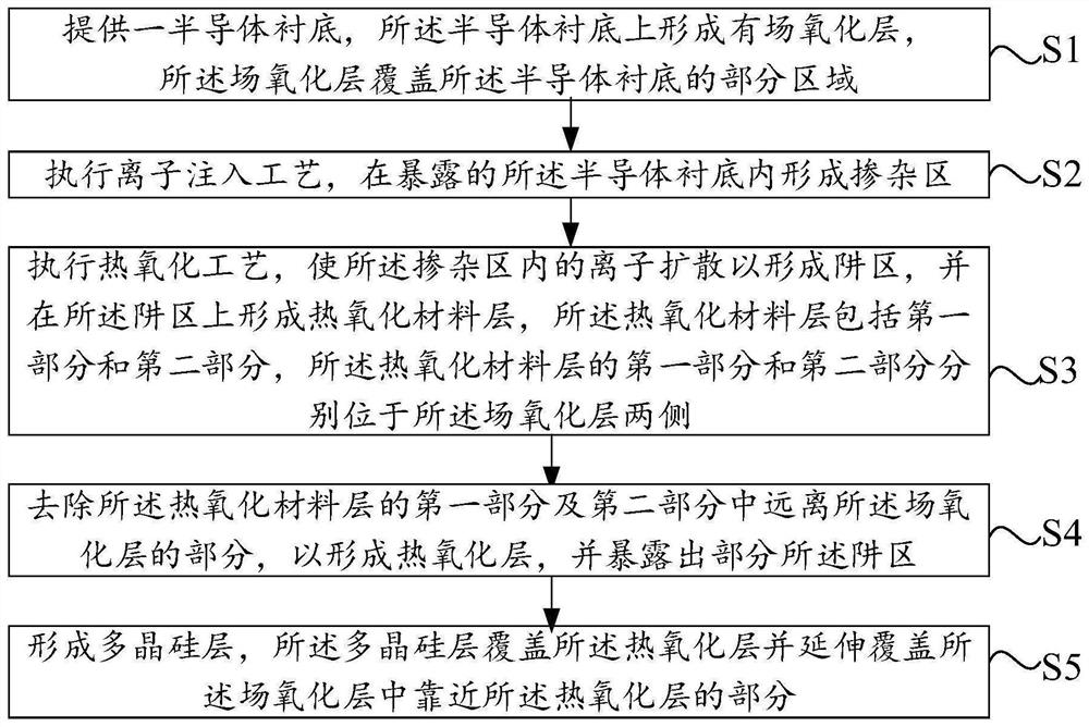
[0035] Please refer to figure 1 , which is a schematic flowchart of a method for manufacturing an insulated gate bipolar transistor provided by an embodiment of the present invention. Such as figure 1 As shown, the manufacturing method of the insulated gate bipolar transistor includes:

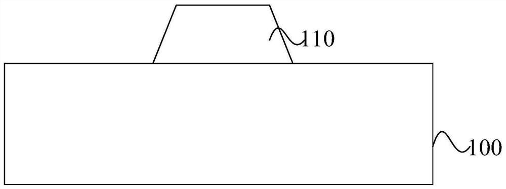
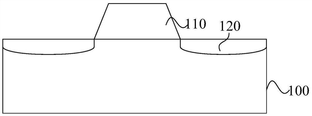
[0036] Step S1: providing a semiconductor substrate, a field oxide layer is formed on the semiconductor substrate, and the field oxide layer covers a part...


PUM


Abstract

The invention provides an insulated gate bipolar transistor and a manufacturing method thereof, and the method comprises the steps: forming a doped region in an exposed semiconductor substrate throughexecuting an ion implantation technology; a thermal oxidation process being executed, ions in the doped region being diffused to form a well region, a thermal oxidation material layer being formed onthe well region, and the thermal oxidation material layer comprising a first part and a second part; then, removing the part, far away from the field oxide layer, of the first part and the second part of the thermal oxide material layer to form a thermal oxide layer; and forming a polycrystalline silicon layer, wherein the polycrystalline silicon layer covers the thermal oxide layer and extends to cover the part, close to the thermal oxide layer, in the field oxide layer. The overall thickness between the polycrystalline silicon layer and the semiconductor substrate can be increased through the thermal oxidation layer, the transistor is prevented from being reversely broken down too early when reverse bias voltage is applied to the transistor, and reverse voltage resistance and high-temperature reliability of the transistor are improved.

Description

technical field [0001] The invention relates to the field of integrated circuit manufacturing, in particular to an insulated gate bipolar transistor and a manufacturing method thereof. Background technique [0002] Insulated Gate Bipolar Transistor (IGBT for short) is a composite fully-controlled voltage-driven power semiconductor device composed of a bipolar transistor (BJT) and an insulated gate field effect transistor (MOSFET). Insulated gate bipolar transistors have the advantages of high input impedance and low conduction voltage drop, so insulated gate bipolar transistors are widely used as an important switching device in various switching circuit structures, such as AC motors, frequency converters, switching power supplies, lighting circuits, traction drives and other fields. For example, insulated gate bipolar transistors are used in circuit structures such as frequency converters and inverters. Among them, the high reverse withstand voltage of the insulated gate ...

Claims


Application Information

Patent Timeline
IPC IPC(8): H01L21/331H01L29/739H01L29/40
CPCH01L29/402H01L29/66325H01L29/7393
Inventor 李娜
Owner SHANGHAI HUAHONG GRACE SEMICON MFG CORP
Why Eureka
Try Eureka